
Datasheet

74AVCH2T45 All information provided in this document is subject to legal disclaimers. © NXP B.V. 2013. All rights reserved.
Product data sheet Rev. 6 — 2 April 2013 5 of 27
NXP Semiconductors
74AVCH2T45
Dual-bit, dual-supply voltage level translator/transceiver; 3-state
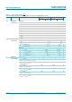
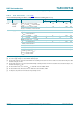
8. Limiting values
[1] The minimum input voltage rating and output voltage ratings may be exceeded if the input and output current ratings are observed.
[2] V
CCO
is the supply voltage associated with the output port.
[3] V
CCO
+ 0.5 V should not exceed 4.6 V.
[4] For VSSOP8 package: above 110 C the value of P
tot
derates linearly with 8 mW/K.
For XSON8 packages: above 118 C the value of P
tot
derates linearly with 7.8 mW/K.
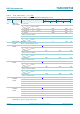
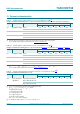
9. Recommended operating conditions
[1] V
CCO
is the supply voltage associated with the output port.
Table 5. Limiting values
In accordance with the Absolute Maximum Rating System (IEC 60134). Voltages are referenced to GND (ground = 0 V).
Symbol Parameter Conditions Min Max Unit
V
CC(A)
supply voltage A 0.5 +4.6 V
V
CC(B)
supply voltage B 0.5 +4.6 V
I
IK
input clamping current V
I
<0V 50 - mA
V
I
input voltage
[1]
0.5 +4.6 V
I
OK
output clamping current V
O
<0V 50 - mA
V
O
output voltage Active mode
[1][2][3]
0.5 V
CCO
+0.5 V
Suspend or 3-state mode
[1]
0.5 +4.6 V
I
O
output current V
O
=0VtoV
CCO
- 50 mA
I
CC
supply current I
CC(A)
or I
CC(B)
-100mA
I
GND
ground current 100 - mA
T
stg
storage temperature 65 +150 C
P
tot
total power dissipation T
amb
= 40 C to +125 C
[4]
-250mW
Table 6. Recommended operating conditions
Symbol Parameter Conditions Min Max Unit
V
CC(A)
supply voltage A 0.8 3.6 V
V
CC(B)
supply voltage B 0.8 3.6 V
V
I
input voltage 0 3.6 V
V
O
output voltage Active mode
[1]
0V
CCO
V
Suspend or 3-state mode 0 3.6 V
T
amb
ambient temperature 40 +125 C
t/V input transition rise and fall rate V
CCI
=0.8 V to 3.6 V - 5 ns/V