
Datasheet


74CBTLV3253 All information provided in this document is subject to legal disclaimers. © NXP B.V. 2011. All rights reserved.
Product data sheet Rev. 4 — 15 December 2011 3 of 19
NXP Semiconductors
74CBTLV3253
Dual 1-of-4 multiplexer/demultiplexer
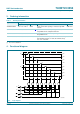
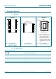
5. Pinning information
5.1 Pinning
5.2 Pin description
(1) This is not a supply pin. The
substrate is attached to this pad
using conductive die attach
material. There is no electrical or
mechanical requirement to
solder this pad. However, if it is
soldered, the solder land should
remain floating or be connected
to GND.
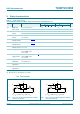
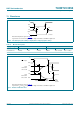
Fig 2. Pin configuration
SOT109-1 (SO16) and
SOT519-1 (SSOP16)
Fig 3. Pin configuration
SOT403-1 (TSSOP16)
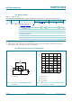
Fig 4. Pin configuration
SOT763-1 (DHVQFN16)
74CBTLV3253
1OE V
CC
S1 2OE
1B4 S0
1B3 2B4
1B2 2B3
1B1 2B2
1A 2B1
GND 2A
001aal209
1
2
3
4
5
6
7
8
10
9
12
11
14
13
16
15
74CBTLV3253
1OE V
CC
S1 2OE
1B4 S0
1B3 2B4
1B2 2B3
1B1 2B2
1A 2B1
GND 2A
001aal210
1
2
3
4
5
6
7
8
10
9
12
11
14
13
16
15
001aal211
74CBTLV3253
1A 2B1
1B1 2B2
1B2 2B3
1B3 2B4
1B4 S0
S1 2OE
GND
2A
1OE
V
CC
Transparent top view
7 10
6 11
5 12
4
13
3 14
2 15
8
9
1
16
terminal 1
index area
GND
(1)
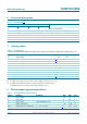
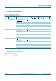
Table 2. Pin description
Symbol Pin Description
1OE
, 2OE 1, 15 output enable input (active LOW)
S0, S1 14, 2 select input
1B1 to 1B4 6, 5, 4, 3 B input/output
2B1 to 2B4 10, 11, 12, 13 B input/output
GND 8 ground (0 V)
1A, 2A 7, 9 A input/output
V
CC
16 supply voltage