
Datasheet


74CBTLV3253 All information provided in this document is subject to legal disclaimers. © NXP B.V. 2011. All rights reserved.
Product data sheet Rev. 4 — 15 December 2011 4 of 19
NXP Semiconductors
74CBTLV3253
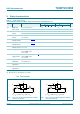
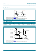
Dual 1-of-4 multiplexer/demultiplexer
6. Functional description
[1] H = HIGH voltage level; L = LOW voltage level.
7. Limiting values
[1] The minimum input voltage rating may be exceeded if the input clamping current ratings are observed.
[2] The switch voltage ratings may be exceeded if switch clamping current ratings are observed
[3] For SSOP16 and TSSOP16 packages: P
tot
derates linearly with 5.5 mW/K above 60 C.
For DHVQFN16 packages: P
tot
derates linearly with 4.5 mW/K above 60 C.
8. Recommended operating conditions
[1] Applies to control signal levels.
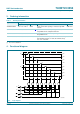
Table 3. Function table
[1]
Inputs Function switch
1OE 2OE S1 S0
X H X X disconnect 2A and 2Bn
HXXXdisconnect 1A and 1Bn
LLLL1A to 1B1 and 2A to 2B1
LLLH1A to 1B2 and 2A to 2B2
L L H L 1A to 1B3 and 2A to 2B3
L L H H 1A to 1B4 and 2A to 2B4
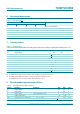
Table 4. Limiting values
In accordance with the Absolute Maximum Rating System (IEC 60134). Voltages are referenced to GND (ground = 0 V).
Symbol Parameter Conditions Min Max Unit
V
CC
supply voltage 0.5 +4.6 V
V
I
input voltage control inputs
[1]
0.5 +4.6 V
V
SW
switch voltage enable and disable mode
[2]
0.5 V
CC
+ 0.5 V
I
IK
input clamping current V
I
< 0.5 V 50 - mA
I
SK
switch clamping current V
I
< 0.5 V 50 - mA
I
SW
switch current V
SW
= 0 V to V
CC
- 128 mA
I
CC
supply current - +100 mA
I
GND
ground current 100 - mA
T
stg
storage temperature 65 +150 C
P
tot
total power dissipation T
amb
= 40 Cto+125C
[3]
- 500 mW
Table 5. Recommended operating conditions
Symbol Parameter Conditions Min Max Unit
V
CC
supply voltage 2.3 3.6 V
V
I
input voltage 0 3.6 V
V
SW
switch voltage enable and disable mode 0 V
CC
V
T
amb
ambient temperature 40 +125 C
t/V input transition rise and fall rate V
CC
= 2.3 V to 3.6 V
[1]
0 200 ns/V