
Datasheet


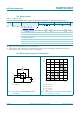

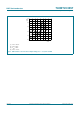

Table Of Contents
- 1. General description
- 2. Features and benefits
- 3. Ordering information
- 4. Functional diagram
- 5. Pinning information
- 6. Functional description
- 7. Limiting values
- 8. Recommended operating conditions
- 9. Static characteristics
- 10. Dynamic characteristics
- 11. Waveforms
- 12. Package outline
- 13. Abbreviations
- 14. Revision history
- 15. Legal information
- 16. Contact information
- 17. Contents

1. General description
The 74CBTLV3257 provides a quad 1-of-2 high-speed multiplexer/demultiplexer with
common select (S) and output enable (OE
) inputs. The low ON resistance of the switch
allows inputs to be connected to outputs without adding propagation delay or generating
additional ground bounce noise. When pin OE
= LOW, one of the two switches is selected
(low-impedance ON-state) with pin S. When pin OE
= HIGH, all switches are in the
high-impedance OFF-state, independent of pin S.
Schmitt trigger action at control input makes the circuit tolerant to slower input rise and fall
times across the entire V
CC
range from 2.3 V to 3.6 V.
To ensure the high-impedance OFF-state during power-up or power-down, OE
should be
tied to the V
CC
through a pull-up resistor. The minimum value of the resistor is determined
by the current-sinking capability of the driver.
This device is fully specified for partial power-down applications using I
OFF
.
The I
OFF
circuitry disables the output, preventing the damaging backflow current through
the device when it is powered down.
2. Features and benefits
Supply voltage range from 2.3 V to 3.6 V
High noise immunity
Complies with JEDEC standard:
JESD8-5 (2.3 V to 2.7 V)
JESD8-B/JESD36 (2.7 V to 3.6 V)
ESD protection:
HBM JESD22-A114F exceeds 2000 V
MM JESD22-A115-A exceeds 200 V
CDM AEC-Q100-011 revision B exceeds 1000 V
5 switch connection between two ports
Rail to rail switching on data I/O ports
CMOS low power consumption
Latch-up performance exceeds 250 mA per JESD78B Class I level A
I
OFF
circuitry provides partial Power-down mode operation
Multiple package options
Specified from 40 Cto+85C and 40 Cto+125C
74CBTLV3257
Quad 1-of-2 multiplexer/demultiplexer
Rev. 4 — 16 December 2011 Product data sheet