
Datasheet


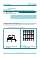

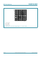

Table Of Contents
- 1. General description
- 2. Features and benefits
- 3. Ordering information
- 4. Functional diagram
- 5. Pinning information
- 6. Functional description
- 7. Limiting values
- 8. Recommended operating conditions
- 9. Static characteristics
- 10. Dynamic characteristics
- 11. Waveforms
- 12. Package outline
- 13. Abbreviations
- 14. Revision history
- 15. Legal information
- 16. Contact information
- 17. Contents

74CBTLV3257 All information provided in this document is subject to legal disclaimers. © NXP B.V. 2011. All rights reserved.
Product data sheet Rev. 4 — 16 December 2011 10 of 19
NXP Semiconductors
74CBTLV3257
Quad 1-of-2 multiplexer/demultiplexer
11. Waveforms
Measurement points are given in Table 9.
Logic levels: V
OL
and V
OH
are typical output voltage levels that occur with the output load.
Fig 14. The data input (nA or nBn) to output (nBn or nA) propagation delays
001aai367
V
M
V
M
V
M
V
M
V
I
input
0 V
V
OH
output
V
OL
t
PHL
t
PLH
Table 9. Measurement points
Supply voltage Input Output
V
CC
V
M
V
I
t
r
= t
f
V
M
V
X
V
Y
2.3 V to 2.7 V 0.5V
CC
V
CC
2.0 ns 0.5V
CC
V
OL
+0.15V V
OH
0.15 V
3.0 V to 3.6 V 0.5V
CC
V
CC
2.0 ns 0.5V
CC
V
OL
+0.3V V
OH
0.3 V
Measurement points are given in Table 9.
Logic levels: V
OL
and V
OH
are typical output voltage levels that occur with the output load.
Fig 15. Enable and disable times
001aal217
t
PLZ
t
PHZ
switch
disabled
switch
enabled
V
Y
V
X
switch
enabled
output
LOW-to-OFF
OFF-to-LOW
output
HIGH-to-OFF
OFF-to-HIGH
OE, S input
V
I
V
CC
V
M
V
M
V
OL
V
OH
GND
GND
t
PZL
t
PZH
V
M
V
M