
Datasheet


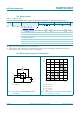

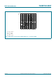
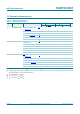

Table Of Contents
- 1. General description
- 2. Features and benefits
- 3. Ordering information
- 4. Functional diagram
- 5. Pinning information
- 6. Functional description
- 7. Limiting values
- 8. Recommended operating conditions
- 9. Static characteristics
- 10. Dynamic characteristics
- 11. Waveforms
- 12. Package outline
- 13. Abbreviations
- 14. Revision history
- 15. Legal information
- 16. Contact information
- 17. Contents
74CBTLV3257 All information provided in this document is subject to legal disclaimers. © NXP B.V. 2011. All rights reserved.
Product data sheet Rev. 4 — 16 December 2011 3 of 19
NXP Semiconductors
74CBTLV3257
Quad 1-of-2 multiplexer/demultiplexer
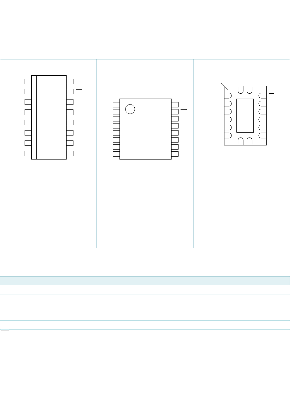
5. Pinning information
5.1 Pinning
5.2 Pin description
(1) This is not a supply pin. The
substrate is attached to this pad
using conductive die attach
material. There is no electrical or
mechanical requirement to
solder this pad. However, if it is
soldered, the solder land should
remain floating or be connected
to GND.
Fig 2. Pin configuration
SOT109-1 (SO16) and
SOT519-1 (SSOP16)
Fig 3. Pin configuration
SOT403-1 (TSSOP16)
Fig 4. Pin configuration
SOT763-1 (DHVQFN16)
74CBTLV3257
SV
CC
1B1 OE
1B2 4B1
1A 4B2
2B1 4A
2B2 3B1
2A 3B2
GND 3A
001aal214
1
2
3
4
5
6
7
8
10
9
12
11
14
13
16
15
74CBTLV3257
SV
CC
1B1 OE
1B2 4B1
1A 4B2
2B1 4A
2B2 3B1
2A 3B2
GND 3A
001aal215
1
2
3
4
5
6
7
8
10
9
12
11
14
13
16
15
001aal216
74CBTLV3257
2A 3B2
2B2 3B1
2B1 4A
1A 4B2
1B2 4B1
1B1 OE
GND
3A
S
V
CC
Transparent top view
7 10
6 11
5 12
4
13
3 14
2 15
8
9
1
16
terminal 1
index area
GND
(1)
Table 2. Pin description
Symbol Pin Description
S 1 select input
1B1 to 4B1 2, 5, 11, 14 B1 input/output
1B2 to 4B2 3, 6, 10, 13 B2 input/output
1A to 4A 4, 7, 9, 12 A input/output
GND 8 ground (0 V)
OE
15 output enable input (active LOW)
V
CC
16 supply voltage