
Datasheet


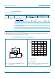

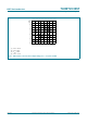

Table Of Contents
- 1. General description
- 2. Features and benefits
- 3. Ordering information
- 4. Functional diagram
- 5. Pinning information
- 6. Functional description
- 7. Limiting values
- 8. Recommended operating conditions
- 9. Static characteristics
- 10. Dynamic characteristics
- 11. Waveforms
- 12. Package outline
- 13. Abbreviations
- 14. Revision history
- 15. Legal information
- 16. Contact information
- 17. Contents
74CBTLV3257 All information provided in this document is subject to legal disclaimers. © NXP B.V. 2011. All rights reserved.
Product data sheet Rev. 4 — 16 December 2011 6 of 19
NXP Semiconductors
74CBTLV3257
Quad 1-of-2 multiplexer/demultiplexer
9.2 ON resistance
[1] Typical values are measured at T
amb
=25C and nominal V
CC
.
[2] Measured by the voltage drop between the A and B terminals at the indicated current through the switch. ON-state resistance is
determined by the lower of the voltages of the two (A or B) terminals.
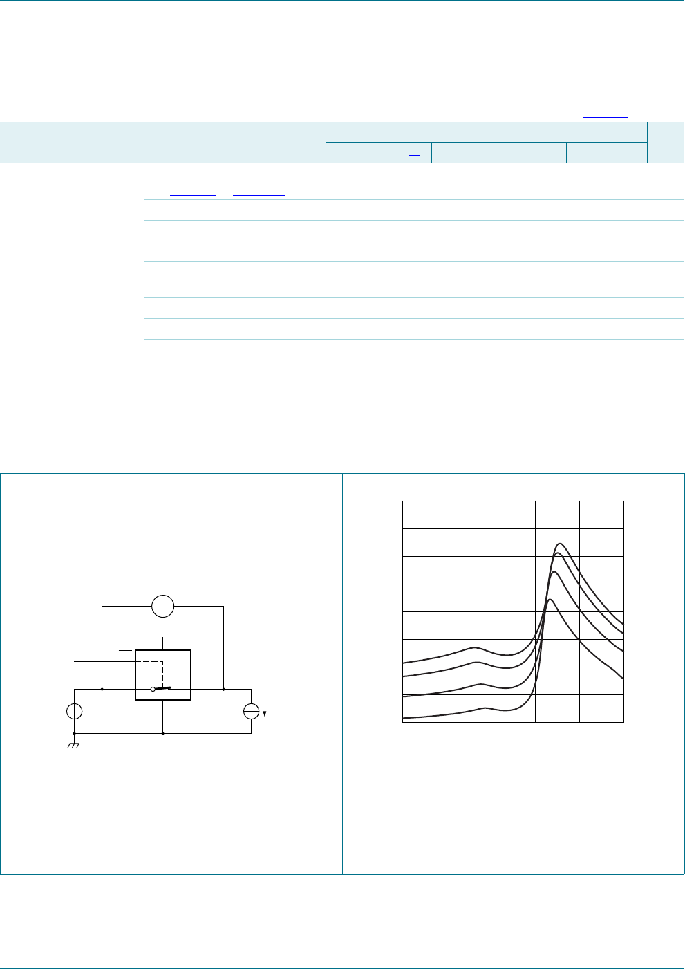
9.3 ON resistance test circuit and graphs
Table 7. Resistance R
ON
At recommended operating conditions; voltages are referenced to GND (ground = 0 V); for test circuit see Figure 7.
Symbol Parameter Conditions T
amb
= 40 C to +85 C T
amb
= 40 C to +125 C Unit
Min Typ
[1]
Max Min Max
R
ON
ON resistance V
CC
= 2.3 V to 2.7 V;
see Figure 8 to Figure 10
[2]
I
SW
=64mA; V
I
= 0 V - 4.2 8.0 - 15.0
I
SW
=24 mA; V
I
= 0 V - 4.2 8.0 - 15.0
I
SW
= 15 mA; V
I
= 1.7 V - 8.4 40.0 - 60.0
V
CC
= 3.0 V to 3.6 V;
see Figure 11
to Figure 13
I
SW
=64mA; V
I
=0V - 4.0 7.0 - 11.0
I
SW
=24 mA; V
I
=0V - 4.0 7.0 - 11.0
I
SW
= 15 mA; V
I
= 2.4 V - 6.2 15.0 - 25.5
R
ON
=V
SW
/ I
SW
.(1)T
amb
= 125 C.
(2) T
amb
= 85 C.
(3) T
amb
= 25 C.
(4) T
amb
= 40 C.
Fig 7. Test circuit for measuring ON resistance
(one switch)
Fig 8. ON resistance as a function of input voltage;
V
CC
= 2.5 V; I
SW
= 15 mA
001aai104
nA
nOE
V
IL
nBn
GND
V
CC
V
l
V
SW
I
SW
V
V
I
(V)
0 2.52.01.0 1.50.5
001aai109
7
5
9
11
R
ON
(Ω)
3
(1)
(3)
(4)
(2)