
Datasheet

74HC_HCT107 All information provided in this document is subject to legal disclaimers. © NXP Semiconductors N.V. 2015. All rights reserved.
Product data sheet Rev. 4 — 26 January 2015 10 of 19
NXP Semiconductors
74HC107; 74HCT107
Dual JK flip-flop with reset; negative-edge trigger
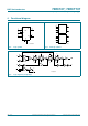
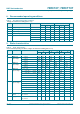
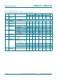
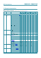
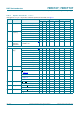
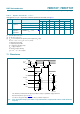
Measurement points are given in Table 8.
V
OL
and V
OH
are typical voltage output levels that occur with the output load.
Fig 6. Reset propagation delays, pulse width and recovery time
DDE
Q4RXWSXW
9
,
*1'
9
,
*1'
9
2+
9
2/
9
2+
9
2/
W
:
Q5LQSXW
9
0
Q4RXWSXW
Q&3LQSXW
9
0
W
UHF
W
3+/
W
3/+
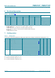
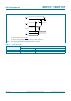
Table 8. Measurement points
Type Input Output
V
I
V
M
V
M
74HC107 V
CC
0.5V
CC
0.5V
CC
74HCT107 3 V 1.3 V 1.3 V