
Datasheet

74HC_HCT107 All information provided in this document is subject to legal disclaimers. © NXP Semiconductors N.V. 2015. All rights reserved.
Product data sheet Rev. 4 — 26 January 2015 3 of 19
NXP Semiconductors
74HC107; 74HCT107
Dual JK flip-flop with reset; negative-edge trigger
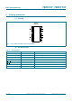
5. Pinning information
5.1 Pinning
5.2 Pin description
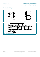
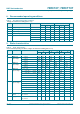
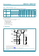
Fig 4. Pin configuration DIP14, SO14 and (T)SSOP14
DDD
+&
+&7
&3
-
5
4
.
4
9
&&
*1
'
&3
.
5
4
-
4
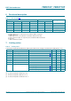
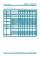
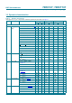
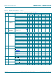
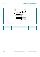
Table 2. Pin description
Symbol Pin Description
1J, 2J 1, 8 synchronous J input
1Q
, 2Q 2, 6 complement output
1Q, 2Q 3, 5 true output
1K, 2K 4, 11 synchronous K input
1CP
, 2CP 12, 9 clock input (HIGH-to-LOW edge-triggered)
1R
, 2R 13, 10 asynchronous reset input (active LOW)
GND 7 ground (0 V)
V
CC
14 supply voltage