
Datasheet

74HC_HCT107 All information provided in this document is subject to legal disclaimers. © NXP Semiconductors N.V. 2015. All rights reserved.
Product data sheet Rev. 4 — 26 January 2015 4 of 19
NXP Semiconductors
74HC107; 74HCT107
Dual JK flip-flop with reset; negative-edge trigger
6. Functional description
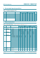
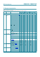
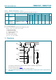
[1] H = HIGH voltage level;
h = HIGH voltage level one set-up time prior to the HIGH-to-LOW clock transition;
L = LOW voltage level;
I = LOW voltage level one set-up time prior to the HIGH-to-LOW clock transition;
q = state of referenced output one set-up time prior to the HIGH-to-LOW clock transition;
X = don’t care;
= HIGH-to-LOW clock transition.
7. Limiting values
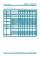
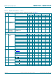
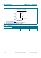
[1] The input and output voltage ratings may be exceeded if the input and output current ratings are observed.
[2] P
tot
derates linearly with 12 mW/K above 70 C.
[3] P
tot
derates linearly with 8 mW/K above 70 C.
[4] P
tot
derates linearly with 5.5 mW/K above 60 C.
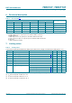
Table 3. Function table
[1]
Input Output Operating mode
R CP J K Q Q
L X X X L H asynchronous reset
H hhq
q toggle
H l h L H load 0 (reset)
H h l H L load 1 (set)
H llqq
hold (no change)
Table 4. Limiting values
In accordance with the Absolute Maximum Rating System (IEC 60134). Voltages are referenced to GND (ground = 0 V).
Symbol Parameter Conditions Min Max Unit
V
CC
supply voltage 0.5 +7.0 V
I
IK
input clamping current V
I
< 0.5 V or V
I
>V
CC
+ 0.5 V
[1]
- 20 mA
I
OK
output clamping current V
O
< 0.5 V or V
O
>V
CC
+0.5V
[1]
- 20 mA
I
O
output current V
O
= 0.5 V to V
CC
+0.5V - 25 mA
I
CC
supply current - 50 mA
I
GND
ground current 50 - mA
T
stg
storage temperature 65 +150 C
P
tot
total power dissipation T
amb
= 40 C to +125 C
DIP14 package
[2]
- 750 mW
SO14 package
[3]
- 500 mW
(T)SSOP14 package
[4]
- 500 mW