
Datasheet

74HC_HCT107 All information provided in this document is subject to legal disclaimers. © NXP Semiconductors N.V. 2015. All rights reserved.
Product data sheet Rev. 4 — 26 January 2015 8 of 19
NXP Semiconductors
74HC107; 74HCT107
Dual JK flip-flop with reset; negative-edge trigger
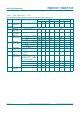
t
h
hold time nJ, nK to nCP; see Figure 5
V
CC
= 2.0 V 3 6- 3 - 3 - ns
V
CC
= 4.5 V 3 2- 3 - 3 - ns
V
CC
= 6.0 V 3 2- 3 - 3 - ns
f
max
maximum
frequency
nCP input; see Figure 5
V
CC
= 2.0 V 6 23 - 4.8 - 4.0 - MHz
V
CC
= 4.5 V 30 70 - 24 - 20 - MHz
V
CC
=5.0V; C
L
=15pF - 78 - - - - - MHz
V
CC
= 6.0 V 35 85 - 28 - 24 - MHz
C
PD
power
dissipation
capacitance
per flip-flop;
V
I
=GNDtoV
CC
[3]
-30- - - - - pF
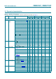
74HCT107
t
pd
propagation
delay
nCP to nQ; see Figure 5
[1]
V
CC
= 4.5 V - 19 36 - 45 - 54 ns
V
CC
=5.0V; C
L
=15pF - 16 - - - - - ns
nCP
to nQ; see Figure 5
V
CC
= 4.5 V - 21 36 - 45 - 54 ns
V
CC
=5.0V; C
L
=15pF - 18 - - - - - ns
nR
to nQ, nQ; see Figure 6
V
CC
= 4.5 V - 20 38 - 48 - 57 ns
V
CC
=5.0V; C
L
=15pF - 17 - - - - - ns
t
t
transition time nQ, nQ; see Figure 5
[2]
V
CC
= 4.5 V - 7 15 - 19 - 22 ns
t
W
pulse width nCP input, HIGH or LOW;
see Figure 5
V
CC
= 4.5 V 16 9 - 20 - 24 - ns
nR
input, HIGH or LOW;
see Figure 6
V
CC
= 4.5 V 20 11 - 25 - 30 - ns
t
rec
recovery time nR to nCP; see Figure 6
V
CC
= 4.5 V 14 8 - 18 - 21 - ns
t
su
set-up time nJ, nK to nCP; see Figure 5
V
CC
= 4.5 V 20 7 - 25 - 30 - ns
t
h
hold time nJ, nK to nCP; see Figure 5
V
CC
= 4.5 V 5 2- 5 - 5 - ns
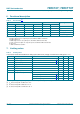
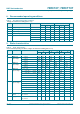
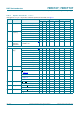
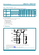
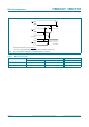
Table 7. Dynamic characteristics
…continued
GND (ground = 0 V); C
L
= 50 pF unless otherwise specified; for test circuit, see Figure 7
Symbol Parameter Conditions 25 C 40 C to +85 C 40 C to +125 C Unit
Min Typ Max Min Max Min Max