
Datasheet

74HC_HCT107 All information provided in this document is subject to legal disclaimers. © NXP Semiconductors N.V. 2015. All rights reserved.
Product data sheet Rev. 4 — 26 January 2015 9 of 19
NXP Semiconductors
74HC107; 74HCT107
Dual JK flip-flop with reset; negative-edge trigger
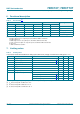
[1] t
pd
is the same as t
PHL
, t
PLH
.
[2] t
t
is the same as t
THL
, t
TLH
.
[3] C
PD
is used to determine the dynamic power dissipation (P
D
in W).
P
D
=C
PD
V
CC
2
f
i
N+(C
L
V
CC
2
f
o
) where:
f
i
= input frequency in MHz;
f
o
= output frequency in MHz;
C
L
= output load capacitance in pF;
V
CC
= supply voltage in V;
N = number of inputs switching;
(C
L
V
CC
2
f
o
) = sum of outputs.
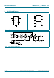
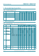
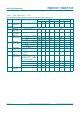
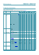
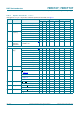
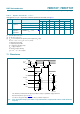
11. Waveforms
f
max
maximum
frequency
nCP input; see Figure 5
V
CC
= 4.5 V 30 66 - 24 - 20 - MHz
V
CC
=5.0V; C
L
=15pF - 73 - - - - - MHz
C
PD
power
dissipation
capacitance
per flip-flop;
V
I
=GNDtoV
CC
1.5 V
[3]
-30- - - - - pF
Table 7. Dynamic characteristics
…continued
GND (ground = 0 V); C
L
= 50 pF unless otherwise specified; for test circuit, see Figure 7
Symbol Parameter Conditions 25 C 40 C to +85 C 40 C to +125 C Unit
Min Typ Max Min Max Min Max
The shaded areas indicate when the input is permitted to change for predictable output performance.
Measurement points are given in Table 8
.
V
OL
and V
OH
are typical voltage output levels that occur with the output load.
Fig 5. Clock propagation delays, pulse width, set-up and hold times, output transition times and the maximum
frequency
W
VX
I
PD[
W
K
Q&3LQSXW
9
0
9
0
W
K
W
VX
W
:
Q-Q.
LQSXW
DDE
Q4RXWSXW
9
,
*1'
9
,
9
2+
9
2/
9
2+
9
2/
*1'
Q4RXWSXW
W
3+/
W
3/+
9
0
W
7/+
W
7+/
W
7/+
9
0
W
7+/
W
3/+
W
3+/