
Datasheet


74HC_HCT154_6 © NXP B.V. 2007. All rights reserved.
Product data sheet Rev. 06 — 12 February 2007 4 of 21
NXP Semiconductors
74HC154; 74HCT154
4-to-16 line decoder/demultiplexer
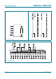
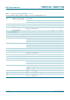
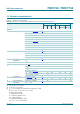
5. Pinning information
5.1 Pinning
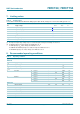
5.2 Pin description
(1) The die substrate is attached to this pad using
conductive die attach material. It cannot be used as
a supply pin or input.
Fig 5. Pin configuration for SO24, DIP24, SSOP24 and
TSSOP24
Fig 6. Pin configuration for DHVQFN24
74HC154D
74HCT154D
74HC154DB
74HCT154DB
74HC154N
74HCT154N
74HC154PW
74HCT154PW
Y0 V
CC
Y1 A0
Y2 A1
Y3 A2
Y4 A3
Y5 E1
Y6 E0
Y7 Y15
Y8 Y14
Y9 Y13
Y10 Y12
GND Y11
001aab067
1
2
3
4
5
6
7
8
9
10
11
12
14
13
16
15
18
17
20
19
22
21
24
23
001aab068
74HC154BQ
74HCT154BQ
Y12
Y9
Y10
Y13
Y8 Y14
Y7 Y15
Y6 E0
Y5 E1
Y4 A3
Y3 A2
Y2 A1
Y1 A0
GND
Y11
Y0
V
CC
11 14
10 15
9 16
817
7 18
6
V
CC
(1)
19
5 20
4 21
3 22
2 23
12
13
1
24
terminal 1
index area
Transparent top view
Table 2. Pin description
Symbol Pin Description
Y0 1 data output (active LOW)
Y1 2 data output (active LOW)
Y2 3 data output (active LOW)
Y3 4 data output (active LOW)
Y4 5 data output (active LOW)
Y5 6 data output (active LOW)
Y6 7 data output (active LOW)
Y7 8 data output (active LOW)
Y8 9 data output (active LOW)
Y9 10 data output (active LOW)
Y10 11 data output (active LOW)
GND 12 ground (0 V)
Y11 13 data output (active LOW)
Y12 14 data output (active LOW)