
Datasheet

December 1990 2
Philips Semiconductors Product specification
Presettable synchronous 4-bit binary
counter; asynchronous reset
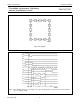
74HC/HCT161
FEATURES
• Synchronous counting and loading
• Two count enable inputs for n-bit cascading
• Positive-edge triggered clock
• Asynchronous reset
• Output capability: standard
• I
CC
category: MSI
GENERAL DESCRIPTION
The 74HC/HCT161 are high-speed Si-gate CMOS devices
and are pin compatible with low power Schottky TTL
(LSTTL). They are specified in compliance with JEDEC
standard no. 7A.
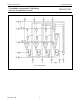
The 74HC/HCT161 are synchronous presettable binary
counters which feature an internal look-ahead carry and
can be used for high-speed counting.
Synchronous operation is provided by having all flip-flops
clocked simultaneously on the positive-going edge of the
clock (CP).
The outputs (Q
0
to Q
3
) of the counters may be preset to a
HIGH or LOW level. A LOW level at the parallel enable
input (PE) disables the counting action and causes the
data at the data inputs (D
0
to D
3
) to be loaded into the
counter on the positive-going edge of the clock (providing
that the set-up and hold time requirements for PE are met).
Preset takes place regardless of the levels at count enable
inputs (CEP and CET).
A LOW level at the master reset input (MR) sets all four
outputs of the flip-flops (Q
0
to Q
3
) to LOW level regardless
of the levels at CP, PE, CET and CEP inputs (thus
providing an asynchronous clear function).
The look-ahead carry simplifies serial cascading of the
counters. Both count enable inputs (CEP and CET) must
be HIGH to count. The CET input is fed forward to enable
the terminal count output (TC). The TC output thus
enabled will produce a HIGH output pulse of a duration
approximately equal to a HIGH level output of Q
0
. This
pulse can be used to enable the next cascaded stage.
The maximum clock frequency for the cascaded counters
is determined by the CP to TC propagation delay and CEP
to CP set-up time, according to the following formula:
f
max
=
1
t
P(max)
(CP to TC) t+
SU
(CEP to CP)
---------------------------------------------------------------------------------------------------
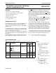
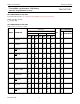
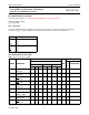
QUICK REFERENCE DATA
GND = 0 V; T
amb
=25°C; t
r
=t
f
= 6 ns
SYMBOL PARAMETER CONDITIONS
TYPICAL
UNIT
HC HCT
t
PHL
/ t
PLH
propagation delay
CP to Q
n
CP to TC
MR to Q
n
MR to TC
CET to TC
C
L
= 15 pF;
V
CC
=5 V 19
21
20
20
10
20
24
25
26
14
ns
ns
ns
ns
ns
f
max
maximum clock frequency 44 45 MHz
C
I
input capacitance 3.5 3.5 pF
C
PD
power dissipation
capacitance per package
notes 1 and 2 33 35 pF
Notes
1. C
PD
is used to determine the
dynamic power dissipation
(P
D
in µW):
P
D
=C
PD
× V
CC
2
× f
i
+
∑ (C
L
× V
CC
2
× f
o
)
where:
f
i
= input frequency in MHz
f
o
= output frequency in MHz
∑ (C
L
× V
CC
2
× f
o
) = sum of
outputs
C
L
= output load capacitance in
pF
V
CC
= supply voltage in V
2. For HC the condition is
V
I
= GND to V
CC
For HCT the condition is
V
I
= GND to V
CC
− 1.5 V