
Datasheet


74HC_HCT164 All information provided in this document is subject to legal disclaimers. © NXP B.V. 2013. All rights reserved.
Product data sheet Rev. 7 — 13 June 2013 10 of 20
NXP Semiconductors
74HC164; 74HCT164
8-bit serial-in, parallel-out shift register
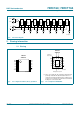
(1) Measurement points are given in Table 8.
V
OL
and V
OH
are typical voltage output levels that occur with the output load.
Fig 8. Waveforms showing the master reset (MR) pulse width, the master reset to output (Qn) propagation
delays and the master reset to clock (CP) removal time
001aac427
MR input
CP input
Qn output
t
PHL
t
W
f
rec
V
M
V
I
GND
V
I
V
OH
V
OL
GND
V
M
V
M
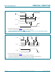
(1) Measurement points are given in Table 8.
V
OL
and V
OH
are typical voltage output levels that occur with the output load.
The shaded areas indicate when the input is permitted to change for predictable output performance.
Fig 9. Waveforms showing the data set-up and hold times for Dn inputs
001aac428
GND
GND
t
h
t
su
t
h
t
su
V
M
V
M
V
M
V
I
V
OH
V
OL
V
I
Qn output
CP input
Dn input