
Datasheet


74HC_HCT164 All information provided in this document is subject to legal disclaimers. © NXP B.V. 2013. All rights reserved.
Product data sheet Rev. 7 — 13 June 2013 3 of 20
NXP Semiconductors
74HC164; 74HCT164
8-bit serial-in, parallel-out shift register
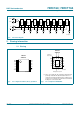
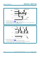
5. Pinning information
5.1 Pinning
Fig 4. Functional diagram
001aac616
Q0
D
FF1
Q
CP
R
D
CP
DSB
DSA
MR
Q1
D
FF2
Q
CP
R
D
Q2
D
FF3
Q
CP
R
D
Q3
D
FF4
Q
CP
R
D
Q4
D
FF5
Q
CP
R
D
Q5
D
FF6
Q
CP
R
D
Q6
D
FF7
Q
CP
R
D
Q7
D
FF8
Q
CP
R
D
(1) This is not a supply pin. The substrate is attached to this
pad using conductive die attach material. There is no
electrical or mechanical requirement to solder this pad.
However, if it is soldered, the solder land should remain
floating or be connected to GND.
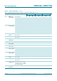
Fig 5. Pin configuration DIP14, SO14, (T)SSOP14 Fig 6. Pin configuration DHVQFN14
74HC164
74HCT164
DSA V
CC
DSB Q7
Q0 Q6
Q1 Q5
Q2 Q4
Q3 MR
GND CP
001aal390
1
2
3
4
5
6
7
8
10
9
12
11
14
13
001aal391
74HC164
74HCT164
GND
(1)
Transparent top view
Q3 MR
Q2 Q4
Q1 Q5
Q0 Q6
DSB Q7
GND
CP
DSA
V
CC
6 9
5 10
4 11
3 12
2 13
7
8
1
14
terminal 1
index area