
Datasheet


74HC_HCT164 All information provided in this document is subject to legal disclaimers. © NXP B.V. 2013. All rights reserved.
Product data sheet Rev. 7 — 13 June 2013 4 of 20
NXP Semiconductors
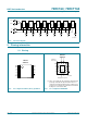
74HC164; 74HCT164
8-bit serial-in, parallel-out shift register
5.2 Pin description
6. Functional description
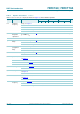
[1] H = HIGH voltage level
h = HIGH voltage level one set-up time prior to the LOW-to-HIGH clock transition
L = LOW voltage level
I = LOW voltage level one set-up time prior to the LOW-to-HIGH clock transition
q = lower case letters indicate the state of the referenced input one set-up time prior to the LOW-to-HIGH clock transition
= LOW-to-HIGH clock transition
7. Limiting values
Table 2. Pin description
Symbol Pin Description
DSA 1 data input
DSB 2 data input
Q0 to Q7 3, 4, 5, 6, 10, 11, 12, 13 output
GND 7 ground (0 V)
CP 8 clock input (LOW-to-HIGH, edge-triggered)
MR
9 master reset input (active LOW)
V
CC
14 positive supply voltage
Table 3. Function table
[1]
Operating
modes
Input Output
MR CP DSA DSB Q0 Q1 to Q7
Reset (clear)LXXXLLtoL
Shift H llLq0to q6
H lhLq0to q6
H hl Lq0to q6
H hhHq0to q6
Table 4. Limiting values
In accordance with the Absolute Maximum Rating System (IEC 60134). Voltages are referenced to GND (ground = 0 V).
Symbol Parameter Conditions Min Max Unit
V
CC
supply voltage 0.5 +7 V
I
IK
input clamping current V
I
< 0.5 V or V
I
>V
CC
+0.5 V
[1]
- 20 mA
I
OK
output clamping current V
O
< 0.5 V or V
O
>V
CC
+0.5V
[1]
- 20 mA
I
O
output current 0.5 V < V
O
< V
CC
+0.5V - 25 mA
I
CC
supply current - 50 mA
I
GND
ground current 50 - mA
T
stg
storage temperature 65 +150 C