
Datasheet

74HC_HCT1G14 All information provided in this document is subject to legal disclaimers. © NXP B.V. 2012. All rights reserved.
Product data sheet Rev. 6 — 27 December 2012 2 of 16
NXP Semiconductors
74HC1G14; 74HCT1G14
Inverting Schmitt trigger
5. Marking
[1] The pin 1 indicator is located on the lower left corner of the device, below the marking code.
6. Functional diagram
7. Pinning information
7.1 Pinning
7.2 Pin description
Table 2. Marking codes
Type number Marking code
[1]
74HC1G14GW HF
74HCT1G14GW TF
74HC1G14GV H14
74HCT1G14GV T14
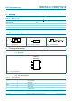
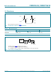
Fig 1. Logic symbol Fig 2. IEC logic symbol Fig 3. Logic diagram
mna023
AY
2
4
24
mna024
mna025
A
Y
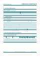
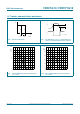
Fig 4. Pin configuration
74HC1G14
74HCT1G14
n.c. V
CC
A
GND Y
001aaf106
1
2
3
5
4
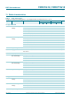
Table 3. Pin description
Symbol Pin Description
n.c. 1 not connected
A 2 data input
GND 3 ground (0 V)
Y 4 data output
V
CC
5 supply voltage