
Datasheet

74HC_HCT240_3 © NXP B.V. 2007. All rights reserved.
Product data sheet Rev. 03 — 2 August 2007 8 of 18
NXP Semiconductors
74HC240; 74HCT240
Octal buffer/line driver; 3-state; inverting
[1] t
pd
is the same as t
PHL
and t
PLH
.
[2] t
en
is the same as t
PZH
and t
PZL
.
[3] t
dis
is the same as t
PHZ
and t
PLZ
.
[4] t
t
is the same as t
THL
and t
TLH
.
[5] C
PD
is used to determine the dynamic power dissipation (P
D
in µW):
P
D
=C
PD
× V
CC
2
× f
i
× N+∑ (C
L
× V
CC
2
× f
o
) where:
f
i
= input frequency in MHz;
f
o
= output frequency in MHz;
C
L
= output load capacitance in pF;
V
CC
= supply voltage in V;
N = number of inputs switching;
∑ (C
L
× V
CC
2
× f
o
) = sum of outputs.
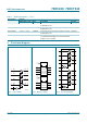
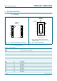
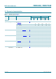
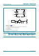
11. Waveforms
74HCT240
t
pd
propagation delay nAn to nYn;
see
Figure 6
[1]
V
CC
= 4.5 V - 11 20 25 30 ns
V
CC
= 5.0 V; C
L
=15pF - 9 - - - ns
t
en
enable time nOE to nYn; V
CC
= 4.5 V; see
Figure 7
[2]
-133038 45ns
t
dis
disable time nOE to nYn; V
CC
= 4.5 V; see
Figure 7
[3]
-132531 38ns
t
t
transition time V
CC
= 4.5 V; see Figure 6
[4]
- 5 12 15 18 ns
C
PD
power dissipation
capacitance
per transceiver;
V
I
= GND to V
CC
− 1.5 V
[5]
-30- - -pF
Table 7. Dynamic characteristics
…continued
GND = 0 V; for load circuit see Figure 8.
Symbol Parameter Conditions 25 °C −40 °C to +125 °C Unit
Min Typ Max Max
(85 °C)
Max
(125 °C)
Measurement points are given in Table 8.
V
OL
and V
OH
are typical voltage output drop that occur with the output load.
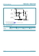
Fig 6. Input (nAn) to output (nYn) propagation delays and output transition times
mgu781
nAn input
nYn output
t
PHL
t
PLH
GND
V
I
V
M
V
M
V
M
V
M
V
OH
V
OL