
Datasheet


74HC_HCT2G17_1 © NXP B.V. 2006. All rights reserved.
Product data sheet Rev. 01 — 6 October 2006 12 of 18
NXP Semiconductors
74HC2G17; 74HCT2G17
Dual non-inverting Schmitt trigger
16. Application information
The slow input rise and fall times cause additional power dissipation, this can be
calculated using the following formula:
P
add
=f
i
× (t
r
×∆I
CC(AV)
+t
f
×∆I
CC(AV)
) × V
CC
where:
P
add
= additional power dissipation (µW);
f
i
= input frequency (MHz);
t
r
= input rise time (ns); 10 % to 90 %;
t
f
= input fall time (ns); 90 % to 10 %;
∆I
CC(AV)
= average additional supply current (µA).
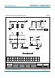
∆I
CC(AV)
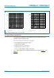
differs with positive or negative input transitions, as shown in Figure 11 and
Figure 12.
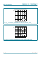
a. V
CC
= 4.5 V. b. V
CC
= 5.5 V.
Fig 10. Typical 74HCT2G17 transfer characteristics
mna031
0 5.0
2.0
0
1.0
I
CC
(mA)
2.5
V
I
(V)
mna032
0
3.0
2.0
1.0
0
3.0 6.0
I
CC
(mA)
V
I
(V)