
Datasheet


74HC_HCT2G17_1 © NXP B.V. 2006. All rights reserved.
Product data sheet Rev. 01 — 6 October 2006 8 of 18
NXP Semiconductors
74HC2G17; 74HCT2G17
Dual non-inverting Schmitt trigger
[1] t
pd
is the same as t
PLH
and t
PHL
[2] t
t
is the same as t
TLH
and t
THL
[3] C
PD
is used to determine the dynamic power dissipation (P
D
in µW).
P
D
=C
PD
× V
CC
2
× f
i
× N+Σ(C
L
× V
CC
2
× f
o
) where:
f
i
= input frequency in MHz;
f
o
= output frequency in MHz;
C
L
= output load capacitance in pF;
V
CC
= supply voltage in V;
N = number of inputs switching;
Σ(C
L
× V
CC
2
× f
o
) = sum of the outputs.
13. Waveforms
74HCT2G17
t
pd
propagation delay nA to nY; see Figure 5
[1]
V
CC
= 4.5 V; C
L
= 50 pF - 21 29 - 36 45 ns
t
t
transition time nY; see Figure 5
[2]
V
CC
= 4.5 V; C
L
= 50 pF - 6 15 - 19 22 ns
C
PD
power dissipation
capacitance
V
I
= GND to V
CC
− 1.5 V
[3]
-10- - - - pF
Table 9. Dynamic characteristics
…continued
Voltages are referenced to GND (ground = 0 V); for test circuit see Figure 6.
Symbol Parameter Conditions 25 °C −40 °C to +125 °C Unit
Min Typ Max Min Max
(85 °C)
Max
(125 °C)
Measurement points are given in Table 10.
V
OL
and V
OH
are typical voltage output drop that occur with the output load.
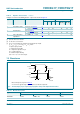
Fig 5. The data input (nA) to output (nY) propagation delays and output transition times
001aaf302
V
I
nA input
t
PLH
V
M
90 % 90 %
10 % 10 %
V
M
t
PHL
t
TLH
t
THL
GND
V
OH
nY output
V
OL
Table 10. Measurement points
Type Input Output
V
M
V
I
t
r
= t
f
V
M
74HC2G17 0.5V
CC
GND to V
CC
6.0 ns 0.5V
CC
74HCT2G17 1.3 V GND to 3.0 V 6.0 ns 1.3 V