
Datasheet


74HC_HCT30 All information provided in this document is subject to legal disclaimers. © NXP B.V. 2012. All rights reserved.
Product data sheet Rev. 6 — 27 December 2012 4 of 16
NXP Semiconductors
74HC30; 74HCT30
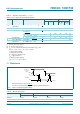
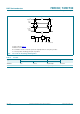
8-input NAND gate
6. Functional description
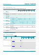
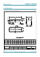
[1] H = HIGH voltage level; L = LOW voltage level; X = don’t care.
7. Limiting values
[1] The input and output voltage ratings may be exceeded if the input and output current ratings are observed.
[2] For DIP14 package: P
tot
derates linearly with 12 mW/K above 70 C.
For SO14 package: P
tot
derates linearly with 8 mW/K above 70 C.
For (T)SSOP14 packages: P
tot
derates linearly with 5.5 mW/K above 60 C.
Table 3. Function table
[1]
Input Output
A B C D E F G H Y
LXXXXXXXH
XLXXXXXXH
XXLXXXXXH
XXXLXXXXH
XXXXLXXXH
XXXXXLXXH
XXXXXXLXH
XXXXXXXLH
HHHHHHHHL
Table 4. Limiting values
In accordance with the Absolute Maximum Rating System (IEC 60134). Voltages are referenced to GND (ground = 0 V).
Symbol Parameter Conditions Min Max Unit
V
CC
supply voltage 0.5 +7 V
I
IK
input clamping current V
I
< 0.5 V or V
I
>V
CC
+0.5 V
[1]
- 20 mA
I
OK
output clamping current V
O
< 0.5 V or V
O
>V
CC
+0.5V
[1]
- 20 mA
I
O
output current 0.5 V < V
O
< V
CC
+0.5V - 25 mA
I
CC
supply current - 50 mA
I
GND
ground current 50 - mA
T
stg
storage temperature 65 +150 C
P
tot
total power dissipation
DIP14 package
[2]
- 750 mW
SO14, (T)SSOP14 packages
[2]
- 500 mW