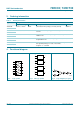
74HC32; 74HCT32 Quad 2-input OR gate Rev. 5 — 4 September 2012 Product data sheet 1. General description The 74HC32; 74HCT32 is a quad 2-input OR gate. Inputs include clamp diodes. This enables the use of current limiting resistors to interface inputs to voltages in excess of VCC. 2. Features and benefits Wide supply voltage range from 2.0 V to 6.
74HC32; 74HCT32 NXP Semiconductors Quad 2-input OR gate 3. Ordering information Table 1. Ordering information Type number 74HC32N Package Temperature range Name Description Version 40 C to +125 C DIP14 plastic dual in-line package; 14 leads (300 mil) SOT27-1 40 C to +125 C SO14 plastic small outline package; 14 leads; body width 3.9 mm SOT108-1 40 C to +125 C SSOP14 plastic shrink small outline package; 14 leads; body width 5.
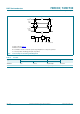
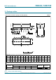
74HC32; 74HCT32 NXP Semiconductors Quad 2-input OR gate 5. Pinning information 1A terminal 1 index area 14 VCC 5.1 Pinning 1 14 VCC 1B 2 13 4B 1B 2 13 4B 12 4A 1Y 3 12 4A 2A 4 32 11 4Y 2B 5 GND(1) 10 3B 2Y 6 1 1A 32 11 4Y 10 3B 2B 5 2Y 6 9 3A GND 7 8 3Y 9 8 4 3Y 2A 7 3 GND 1Y 3A 001aad102 Transparent top view 001aad101 (1) The die substrate is attached to this pad using conductive die attach material. It cannot be used as a supply pin or input. Fig 4.
74HC32; 74HCT32 NXP Semiconductors Quad 2-input OR gate 7. Limiting values Table 4. Limiting values In accordance with the Absolute Maximum Rating System (IEC 60134). Voltages are referenced to GND (ground = 0 V). Symbol Parameter VCC supply voltage Conditions Min Max Unit 0.5 +7 V - 20 mA - 20 mA - 25 mA 50 mA IIK input clamping current VI < 0.5 V or VI > VCC + 0.5 V [1] IOK output clamping current VO < 0.5 V or VO > VCC + 0.5 V [1] IO output current 0.
74HC32; 74HCT32 NXP Semiconductors Quad 2-input OR gate 9. Static characteristics Table 6. Static characteristics At recommended operating conditions; voltages are referenced to GND (ground = 0 V). Symbol Parameter 25 C Conditions Min Typ VCC = 2.0 V 1.5 VCC = 4.5 V 40 C to +85 C 40 C to +125 C Unit Max Min Max Min Max 1.2 - 1.5 - 1.5 - V 3.15 2.4 - 3.15 - 3.15 - V VCC = 6.0 V 4.2 3.2 - 4.2 - 4.
74HC32; 74HCT32 NXP Semiconductors Quad 2-input OR gate Table 6. Static characteristics …continued At recommended operating conditions; voltages are referenced to GND (ground = 0 V). Symbol Parameter 25 C Conditions Min 40 C to +85 C 40 C to +125 C Unit Typ Max Min Max Min Max ICC supply current VI = VCC or GND; IO = 0 A; VCC = 5.5 V - - 2.0 - 20 - 40 A ICC additional supply current per input pin; VI = VCC 2.1 V; IO = 0 A; other inputs at VCC or GND; VCC = 4.5 V to 5.
4HC32; 74HCT32 NXP Semiconductors Quad 2-input OR gate Table 7. Dynamic characteristics GND = 0 V; CL = 50 pF; for load circuit see Figure 7. Symbol Parameter 25 C Conditions 40 C to +125 C Unit Min Typ Max Max (85 C) Max (125 C) - 11 24 30 36 ns - 9 - - - ns 74HCT32 [1] propagation delay nA, nB to nY; see Figure 6 tpd VCC = 4.5 V VCC = 5.0 V; CL = 15 pF tt transition time VCC = 4.
74HC32; 74HCT32 NXP Semiconductors Quad 2-input OR gate VI negative pulse tW 90 % VM VM 10 % GND tr tf tr tf VI 90 % positive pulse GND VM VM 10 % tW VCC G VI VO DUT RT CL 001aah768 Test data is given in Table 9. Definitions test circuit: RT = termination resistance should be equal to output impedance Zo of the pulse generator. CL = load capacitance including jig and probe capacitance. Fig 7. Table 9.
74HC32; 74HCT32 NXP Semiconductors Quad 2-input OR gate 12. Package outline DIP14: plastic dual in-line package; 14 leads (300 mil) SOT27-1 ME seating plane D A2 A A1 L c e Z w M b1 (e 1) b MH 8 14 pin 1 index E 1 7 0 5 10 mm scale DIMENSIONS (inch dimensions are derived from the original mm dimensions) UNIT A max. A1 min. A2 max. b b1 c D (1) E (1) e e1 L ME MH w Z (1) max. mm 4.2 0.51 3.2 1.73 1.13 0.53 0.38 0.36 0.23 19.50 18.55 6.48 6.20 2.54 7.62 3.
74HC32; 74HCT32 NXP Semiconductors Quad 2-input OR gate SO14: plastic small outline package; 14 leads; body width 3.9 mm SOT108-1 D E A X c y HE v M A Z 8 14 Q A2 A (A 3) A1 pin 1 index θ Lp 1 L 7 e detail X w M bp 0 2.5 5 mm scale DIMENSIONS (inch dimensions are derived from the original mm dimensions) UNIT A max. A1 A2 A3 bp c D (1) E (1) e HE L Lp Q v w y Z (1) mm 1.75 0.25 0.10 1.45 1.25 0.25 0.49 0.36 0.25 0.19 8.75 8.55 4.0 3.8 1.27 6.2 5.8 1.
74HC32; 74HCT32 NXP Semiconductors Quad 2-input OR gate SSOP14: plastic shrink small outline package; 14 leads; body width 5.3 mm D SOT337-1 E A X c y HE v M A Z 8 14 Q A2 A (A 3) A1 pin 1 index θ Lp L 7 1 detail X w M bp e 0 2.5 5 mm scale DIMENSIONS (mm are the original dimensions) UNIT A max. A1 A2 A3 bp c D (1) E (1) e HE L Lp Q v w y Z (1) θ mm 2 0.21 0.05 1.80 1.65 0.25 0.38 0.25 0.20 0.09 6.4 6.0 5.4 5.2 0.65 7.9 7.6 1.25 1.03 0.63 0.9 0.7 0.
74HC32; 74HCT32 NXP Semiconductors Quad 2-input OR gate TSSOP14: plastic thin shrink small outline package; 14 leads; body width 4.4 mm SOT402-1 E D A X c y HE v M A Z 8 14 Q (A 3) A2 A A1 pin 1 index θ Lp L 1 7 e detail X w M bp 0 2.5 5 mm scale DIMENSIONS (mm are the original dimensions) UNIT A max. A1 A2 A3 bp c D (1) E (2) e HE L Lp Q v w y Z (1) θ mm 1.1 0.15 0.05 0.95 0.80 0.25 0.30 0.19 0.2 0.1 5.1 4.9 4.5 4.3 0.65 6.6 6.2 1 0.75 0.50 0.
74HC32; 74HCT32 NXP Semiconductors Quad 2-input OR gate DHVQFN14: plastic dual in-line compatible thermal enhanced very thin quad flat package; no leads; SOT762-1 14 terminals; body 2.5 x 3 x 0.85 mm A B D A A1 E c detail X terminal 1 index area terminal 1 index area C e1 e 2 6 y y1 C v M C A B w M C b L 1 7 Eh e 14 8 13 9 Dh X 0 2.5 5 mm scale DIMENSIONS (mm are the original dimensions) UNIT mm A(1) max. A1 b 1 0.05 0.00 0.30 0.18 c D (1) Dh E (1) Eh 0.2 3.1 2.
74HC32; 74HCT32 NXP Semiconductors Quad 2-input OR gate 13. Abbreviations Table 10. Abbreviations Acronym Description CMOS Complementary Metal-Oxide Semiconductor DUT Device Under Test ESD ElectroStatic Discharge HBM Human Body Model LSTTL Low-power Schottky Transistor-Transistor Logic MM Machine Model TTL Transistor-Transistor Logic 14. Revision history Table 11. Revision history Document ID Release date Data sheet status Change notice Supersedes 74HC_HCT32 v.
74HC32; 74HCT32 NXP Semiconductors Quad 2-input OR gate 15. Legal information 15.1 Data sheet status Document status[1][2] Product status[3] Definition Objective [short] data sheet Development This document contains data from the objective specification for product development. Preliminary [short] data sheet Qualification This document contains data from the preliminary specification. Product [short] data sheet Production This document contains the product specification.
74HC32; 74HCT32 NXP Semiconductors Quad 2-input OR gate Export control — This document as well as the item(s) described herein may be subject to export control regulations. Export might require a prior authorization from competent authorities. Non-automotive qualified products — Unless this data sheet expressly states that this specific NXP Semiconductors product is automotive qualified, the product is not suitable for automotive use.
74HC32; 74HCT32 NXP Semiconductors Quad 2-input OR gate 17. Contents 1 2 3 4 5 5.1 5.2 6 7 8 9 10 11 12 13 14 15 15.1 15.2 15.3 15.4 16 17 General description . . . . . . . . . . . . . . . . . . . . . . 1 Features and benefits . . . . . . . . . . . . . . . . . . . . 1 Ordering information . . . . . . . . . . . . . . . . . . . . . 2 Functional diagram . . . . . . . . . . . . . . . . . . . . . . 2 Pinning information . . . . . . . . . . . . . . . . . . . . . . 3 Pinning . . . . . . . . . . . . . . . . . .