
Datasheet

74HC_HCT373_Q100 All information provided in this document is subject to legal disclaimers. © NXP B.V. 2012. All rights reserved.
Product data sheet Rev. 1 — 10 August 2012 15 of 24
NXP Semiconductors
74HC373-Q100; 74HCT373-Q100
Octal D-type transparent latch; 3-state
[1] t
pd
is the same as t
PLH
and t
PHL
.
[2] t
en
is the same as t
PZH
and t
PZL
.
[3] t
dis
is the same as t
PLZ
and t
PHZ
.
[4] t
t
is the same as t
THL
and t
TLH
.
[5] C
PD
is used to determine the dynamic power dissipation (P
D
in W).
P
D
=C
PD
V
CC
2
f
i
N+(C
L
V
CC
2
f
o
) where:
f
i
= input frequency in MHz;
f
o
= output frequency in MHz;
C
L
= output load capacitance in pF;
V
CC
= supply voltage in V;
N = number of inputs switching;
(C
L
V
CC
2
f
o
) = sum of outputs.
11. Waveforms
t
h
hold time Dn to LE Dn to LE; see Figure 11
V
CC
= 4.5 V 4 - - ns
Table 9. Dynamic characteristics 74HCT373-Q100
…continued
Voltages are referenced to GND (ground = 0 V); C
L
= 50 pF unless otherwise specified; for test circuit see Figure 12.
Symbol Parameter Conditions Min Typ Max Unit
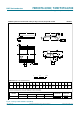
Measurement points are given in Table 10.
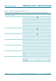
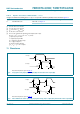
Fig 8. Propagation delay input (Dn) to output (Qn) and transition time output (Qn)
001aae082
Dn input
Qn output
V
M
t
PLH
t
PHL
t
THL
t
TLH
V
M
90 %
10 %
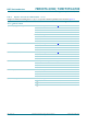
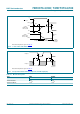
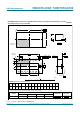
Measurement points are given in Table 10.
Fig 9. Pulse width latch enable input (LE), propagation delay (LE) to output (Qn) and transition time output (Qn)
V
M
V
M
t
PLH
t
PHL
t
W
LE input
Qn output
001aae083
t
TLH
t
THL
90 %
10 %