
Datasheet


74HC_HCT373_Q100 All information provided in this document is subject to legal disclaimers. © NXP B.V. 2012. All rights reserved.
Product data sheet Rev. 1 — 10 August 2012 4 of 24
NXP Semiconductors
74HC373-Q100; 74HCT373-Q100
Octal D-type transparent latch; 3-state
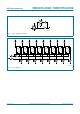
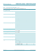
5. Pinning information
5.1 Pinning
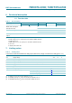
5.2 Pin description
(1) The die substrate is attached to this pad using
conductive die attach material. It cannot be used as
supply pin or input.
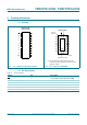
Fig 6. Pin configuration SO20 and TSSOP20 Fig 7. Pin configuration DHVQFN20
+&4
+&74
9
&&
4
'
'
4
4
'
'
4
/(
DDD
2
(
4
'
'
4
4
'
'
4
*1
'
+&4
+&74
4
'
'
4
4
'
'
*1'
4
*1'
/(
2(
9
&&
WHU
PLQDO
LQG
H[DUHD
'
4
'
4
4
'
'
4
7UDQVSDUHQWWRSYLHZ
DDD
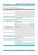
Table 2. Pin description
Symbol Pin Description
OE
1 3-state output enable input (active LOW)
Q0, Q1, Q2, Q3, Q4, Q5, Q6, Q7 2, 5, 6, 9, 12, 15, 16, 19 3-state latch output
D0, D1, D2, D3, D4, D5, D6, D7 3, 4, 7, 8, 13, 14, 17, 18 data input
GND 10 ground (0 V)
LE 11 latch enable input (active HIGH)
V
CC
20 supply voltage