
Datasheet


74HC_HCT373_Q100 All information provided in this document is subject to legal disclaimers. © NXP B.V. 2012. All rights reserved.
Product data sheet Rev. 1 — 10 August 2012 5 of 24
NXP Semiconductors
74HC373-Q100; 74HCT373-Q100
Octal D-type transparent latch; 3-state
6. Functional description
6.1 Function table
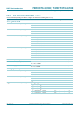
[1] H = HIGH voltage level;
h = HIGH voltage level one set-up time prior to the HIGH-to-LOW LE transition;
L = LOW voltage level;
I = LOW voltage level one set-up time prior to the HIGH-to-LOW LE transition;
X = don’t care;
Z = high-impedance OFF-state.
7. Limiting values
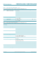
[1] For SO20: P
tot
derates linearly with 8 mW/K above 70 C.
[2] For TSSOP20 packages: P
tot
derates linearly with 5.5 mW/K above 60 C.
[3] For DHVQFN20 package: P
tot
derates linearly with 4.5 mW/K above 60 C.
Table 3. Function table
[1]
Operating mode Control Input Internal latches Output
OE LE Dn Qn
Enable and read register
(transparent mode)
LHLL L
HH H
Latch and read register L L l L L
hH H
Latch register and disable
outputs
HXXX Z
Table 4. Limiting values
In accordance with the Absolute Maximum Rating System (IEC 60134). Voltages are referenced to GND (ground = 0 V).
Symbol Parameter Conditions Min Max Unit
V
CC
supply voltage 0.5 +7 V
I
IK
input clamping current V
I
< 0.5 V or V
I
>V
CC
+0.5 V - 20 mA
I
OK
output clamping current V
O
< 0.5 V or V
O
>V
CC
+0.5V - 20 mA
I
O
output current V
O
= 0.5 V to (V
CC
+0.5V) - 35 mA
I
CC
supply current - +70 mA
I
GND
ground current - 70 mA
T
stg
storage temperature 65 +150 C
P
tot
total power dissipation SO20 package
[1]
- 500 mW
TSSOP20 package
[2]
500 mW
DHVQFN20 package
[3]
- 500 mW