
Datasheet

74HC_HCT377 All information provided in this document is subject to legal disclaimers. © NXP B.V. 2013. All rights reserved.
Product data sheet Rev. 3 — 25 September 2013 4 of 19
NXP Semiconductors
74HC377; 74HCT377
Octal D-type flip-flop with data enable; positive-edge trigger
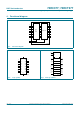
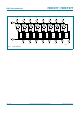
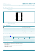
5. Pinning information
5.1 Pinning
5.2 Pin description
6. Functional description
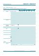
[1] H = HIGH voltage level;
h = HIGH voltage level one set-up time prior to the LOW-to-HIGH clock transition;
L = LOW voltage level;
l = LOW voltage level one set-up time prior to the LOW-to-HIGH clock transition;
X = don’t care;
= LOW-to-HIGH clock transition.
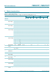
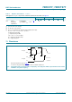
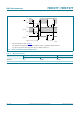
Fig 5. Pin configuration
377
EV
CC
Q0 Q7
D0 D7
D1 D6
Q1 Q6
Q2 Q5
D2 D5
D3 D4
Q3 Q4
GND CP
mna917
1
2
3
4
5
6
7
8
9
10
12
11
14
13
16
15
18
17
20
19
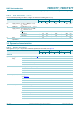
Table 2. Pin description
Symbol Pin Description
E
1 data enable input (active LOW)
Q0, Q1, Q2, Q3, Q4, Q5, Q6, Q7 2, 5, 6, 9, 12, 15, 16, 19 flip-flop output
D0, D1, D2, D3, D4, D5, D6, D7 3, 4, 7, 8, 13, 14, 17, 18 data input
GND 10 ground (0 V)
CP 11 clock input (LOW-to-HIGH, edge triggered)
V
CC
20 supply voltage
Table 3. Function table
[1]
Operating modes Inputs Outputs
CP E Dn Qn
load “1” lhH
load “0” llL
hold (do nothing) h X no change
X H X no change