
Datasheet

74HC_HCT377 All information provided in this document is subject to legal disclaimers. © NXP B.V. 2013. All rights reserved.
Product data sheet Rev. 3 — 25 September 2013 9 of 19
NXP Semiconductors
74HC377; 74HCT377
Octal D-type flip-flop with data enable; positive-edge trigger
[1] t
pd
is the same as t
PHL
and t
PLH
.
[2] t
t
is the same as t
THL
and t
TLH
.
[3] C
PD
is used to determine the dynamic power dissipation (P
D
in W).
P
D
= C
PD
V
CC
2
f
i
+ (C
L
V
CC
2
f
o
) where:
f
i
= input frequency in MHz;
f
o
= output frequency in MHz;
(C
L
V
CC
2
f
o
) = sum of outputs;
C
L
= output load capacitance in pF;
V
CC
= supply voltage in V.
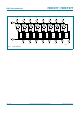
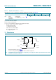
11. Waveforms
C
PD
power
dissipation
capacitance
per package;
V
I
=GNDtoV
CC
1.5 V
[3]
-20- - - - - pF
Table 7. Dynamic characteristics
…continued
GND (ground = 0 V); C
L
= 50 pF unless otherwise specified; for test circuit, see Figure 8
Symbol Parameter Conditions 25 C 40 C to +85 C 40 C to +125 C Unit
Min Typ Max Min Max Min Max
Measurement points are given in Table 8.
V
OL
and V
OH
are typical voltage output levels that occur with the output load.
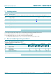
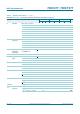
Fig 6. Propagation delay clock input (CP) to output (Qn), clock (CP) pulse width, output transition time and the
maximum clock pulse frequency
001aac426
CP input
Qn
output
t
PHL
t
PLH
t
W
V
OH
V
I
GND
V
OL
V
M
V
M
1/f
max