
Datasheet


74HC3GU04 All information provided in this document is subject to legal disclaimers. © NXP B.V. 2013. All rights reserved.
Product data sheet Rev. 5 — 2 October 2013 5 of 17
NXP Semiconductors 74HC3GU04
Triple unbuffered inverter
[1] All typical values are measured at T
amb
= 25 C.
[2] t
pd
is the same as t
PLH
and t
PHL
.
[3] t
t
is the same as t
TLH
and t
THL
.
[4] C
PD
is used to determine the dynamic power dissipation (P
D
in W).
P
D
= C
PD
V
CC
2
f
i
N + (C
L
V
CC
2
f
o
) where:
f
i
= input frequency in MHz;
f
o
= output frequency in MHz;
C
L
= output load capacitance in pF;
V
CC
= supply voltage in V;
N = number of inputs switching;
(C
L
V
CC
2
f
o
) = sum of outputs.
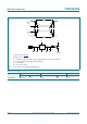
12. Waveforms
t
t
transition time nY; see Figure 5
[3]
V
CC
= 2.0 V - 18 95 - 125 ns
V
CC
= 4.5 V - 6 19 - 25 ns
V
CC
= 6.0 V - 5 16 - 20 ns
C
PD
power dissipation
capacitance
V
I
=GNDtoV
CC
[4]
-5-- -pF
Table 8. Dynamic characteristics
…continued
Voltages are referenced to GND (ground = 0 V); for test circuit see Figure 6.
Symbol Parameter Conditions 40 C to +85 C 40 C to +125 C Unit
Min Typ
[1]
Max Min Max
Measurement points are given in Table 9.
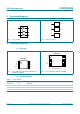
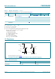
Fig 5. Propagation delay data input (nA) to data output (nY) and transition time output (nY)
mna722
t
PLH
t
PHL
V
M
V
M
90 %
10 %
V
M
V
M
nY output
nA input
V
I
GND
V
OH
V
OL
t
TLH
t
THL
Table 9. Measurement points
Type Input Output
V
M
V
M
74HC3GU04 0.5 V
CC
0.5 V
CC