
Datasheet


1997 Nov 25 3
Philips Semiconductors Product specification
Phase-locked-loop with VCO 74HC/HCT4046A
The frequency capture range (2f
c
) is defined as the
frequency range of input signals on which the PLL will lock
if it was initially out-of-lock. The frequency lock range
(2f
L
) is defined as the frequency range of input signals on
which the loop will stay locked if it was initially in lock. The
capture range is smaller or equal to the lock range.
With PC1, the capture range depends on the low-pass
filter characteristics and can be made as large as the lock
range.
This configuration retains lock even with very noisy input
signals. Typical behaviour of this type of phase
comparator is that it can lock to input frequencies close to
the harmonics of the VCO centre frequency.
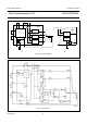
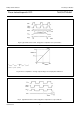
Phase comparator 2 (PC2)
This is a positive edge-triggered phase and frequency
detector. When the PLL is using this comparator, the loop
is controlled by positive signal transitions and the duty
factors of SIG
IN
and COMP
IN
are not important. PC2
comprises two D-type flip-flops, control-gating and a
3-state output stage. The circuit functions as an up-down
counter (Fig.5) where SIG
IN
causes an up-count and
COMP
IN
a down-count. The transfer function of PC2,
assuming ripple (f
r
=f
i
) is suppressed,
is:
where V
DEMOUT
is the demodulator output at pin 10;
V
DEMOUT
=V
PC2OUT
(via low-pass filter).
The phase comparator gain is:
V
DEMOUT
is the resultant of the initial phase differences of
SIG
IN
and COMP
IN
as shown in Fig.8. Typical waveforms
for the PC2 loop locked at f
o
are shown in Fig.9.
When the frequencies of SIG
IN
and COMP
IN
are equal but
the phase of SIG
IN
leads that of COMP
IN
, the p-type
output driver at PC2
OUT
is held “ON” for a time
corresponding to the phase difference (φ
DEMOUT
). When
the phase of SIG
IN
lags that of COMP
IN
, the n-type driver
is held “ON”.
When the frequency of SIG
IN
is higher than that of
COMP
IN
, the p-type output driver is held “ON” for most of
the input signal cycle time, and for the remainder of the
cycle both n and p- type drivers are ”OFF” (3-state). If the
SIG
IN
frequency is lower than the COMP
IN
frequency, then
it is the n-type driver that is held “ON” for most of the cycle.
Subsequently, the voltage at the capacitor (C2) of the
low-pass filter connected to PC2
OUT
varies until the signal
V
DEMOUT
V
CC
4π
-----------
φ
SIGIN
φ
COMPIN
–()=
K
p
V
CC
4π
-----------
Vr⁄().=
and comparator inputs are equal in both phase and
frequency. At this stable point the voltage on C2 remains
constant as the PC2 output is in 3-state and the VCO input
at pin 9 is a high impedance. Also in this condition, the
signal at the phase comparator pulse output (PCP
OUT
) is a
HIGH level and so can be used for indicating a locked
condition.
Thus, for PC2, no phase difference exists between
SIG
IN
and COMP
IN
over the full frequency range of the
VCO. Moreover, the power dissipation due to the low-pass
filter is reduced because both p and n-type drivers are
“OFF” for most of the signal input cycle. It should be noted
that the PLL lock range for this type of phase comparator
is equal to the capture range and is independent of the
low-pass filter. With no signal present at SIG
IN
the
VCO adjusts, via PC2, to its lowest frequency.
Phase comparator 3 (PC3)
This is a positive edge-triggered sequential phase detector
using an RS-type flip-flop. When the PLL is using this
comparator, the loop is controlled by positive signal
transitions and the duty factors of SIG
IN
and COMP
IN
are
not important. The transfer characteristic of PC3,
assuming ripple (f
r
=f
i
) is suppressed,
is:
where V
DEMOUT
is the demodulator output at pin 10;
V
DEMOUT
=V
PC3OUT
(via low-pass filter).
The phase comparator gain is:
The average output from PC3, fed to the VCO via the
low-pass filter and seen at the demodulator output at
pin 10 (V
DEMOUT
), is the resultant of the phase differences
of SIG
IN
and COMP
IN
as shown in Fig.10. Typical
waveforms for the PC3 loop locked at f
o
are shown in
Fig.11.
The phase-to-output response characteristic of PC3
(Fig.10) differs from that of PC2 in that the phase angle
between SIG
IN
and COMP
IN
varies between 0° and
360° and is 180° at the centre frequency. Also PC3 gives
a greater voltage swing than PC2 for input phase
differences but as a consequence the ripple content of the
VCO input signal is higher. The PLL lock range for this type
of phase comparator and the capture range are dependent
on the low-pass filter. With no signal present at SIG
IN
the
VCO adjusts, via PC3, to its lowest frequency.
V
DEMOUT
V
CC
2π
-----------
φ
SIGIN
φ
COMPIN
–()=
K
p
V
CC
2π
-----------
Vr⁄().=