
Datasheet


December 1990 2
Philips Semiconductors Product specification
Hex high-to-low level shifter 74HC4050
FEATURES
• Output capability: standard
• I
CC
category: SSI
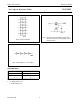
GENERAL DESCRIPTION
The 74HC4050 is a high-speed Si-gate CMOS device and
is pin compatible with the “4050” of the “4000B” series. It
is specified in compliance with JEDEC standard no. 7A.
The 74HC4050 provides six non-inverting buffers with a
modified input protection structure, which has no diode
connected to V
CC
. Input voltages of up to 15 V may
therefore be used. This feature enables the non-inverting
buffers to be used as logic level translators, which will
convert high level logic to low level logic, while operating
from a low voltage power supply. For example 15 V logic
(“4000B series”) can be converted down to 2 V logic.
The actual input switch level remains related to the V
CC
and is the same as mentioned in the family characteristics.
APPLICATIONS
• Converting 15 V logic (“4000B” series) down to 2 V logic.
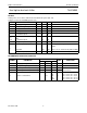
QUICK REFERENCE DATA
GND = 0 V; T
amb
=25°C; t
r
=t
f
= 6 ns
Notes
1. C
PD
is used to determine the dynamic power dissipation (P
D
in µW):
P
D
=C
PD
× V
CC
2
× f
i
+∑ (C
L
× V
CC
2
× f
o
) where:
f
i
= input frequency in MHz
f
o
= output frequency in MHz
C
L
= output load capacitance in pF
V
CC
= supply voltage in V
∑ (C
L
× V
CC
2
× f
o
) = sum of outputs
ORDERING INFORMATION
See
“74HC/HCT/HCU/HCMOS Logic Package Information”
.
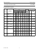
SYMBOL PARAMETER CONDITIONS
TYPICAL
UNIT
HC
t
PHL
/ t
PLH
propagation delay nA to nY C
L
= 15 pF; V
CC
= 5 V 7 ns
C
I
input capacitance 3.5 pF
C
PD
power dissipation capacitance per buffer note 1 14 pF