
Datasheet


74HC_HCT4052 All information provided in this document is subject to legal disclaimers. © NXP B.V. 2012. All rights reserved.
Product data sheet Rev. 10 — 19 July 2012 16 of 29
NXP Semiconductors
74HC4052; 74HCT4052
Dual 4-channel analog multiplexer/demultiplexer
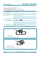
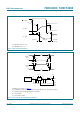
For 74HC4052: V
M
=0.5 V
CC
.
For 74HCT4052: V
M
=1.3V.
Fig 14. Turn-on and turn-off times
001aae330
t
PLZ
t
PHZ
switch OFF
switch ON
switch ON
V
os
output
V
os
output
E, Sn inputs
V
M
V
I
0 V
90 %
10 %
t
PZL
t
PZH
50 %
50 %
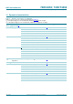
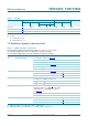
Definitions for test circuit; see Table 11:
R
T
= termination resistance should be equal to the output impedance Z
o
of the pulse generator.
C
L
= load capacitance including jig and probe capacitance.
R
L
= load resistance.
S1 = Test selection switch.
Fig 15. Test circuit for measuring AC performance
V
M
V
M
t
W
t
W
10 %
90 %
0 V
V
I
V
I
negative
pulse
positive
pulse
0 V
V
M
V
M
90 %
10 %
t
f
t
r
t
r
t
f
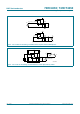
001aae382
V
CC
V
CC
open
GND
V
EE
V
I
V
os
DUT
C
L
R
T
R
L
S1
PULSE
GENERATOR
V
is