74HC595; 74HCT595 8-bit serial-in, serial or parallel-out shift register with output latches; 3-state Rev. 7 — 26 January 2015 Product data sheet 1. General description The 74HC595; 74HCT595 are high-speed Si-gate CMOS devices and are pin compatible with Low-power Schottky TTL (LSTTL). They are specified in compliance with JEDEC standard No. 7A. The 74HC595; 74HCT595 are 8-stage serial shift registers with a storage register and 3-state outputs. The registers have separate clocks.
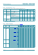
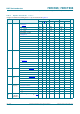
74HC595; 74HCT595 NXP Semiconductors 8-bit serial-in, serial or parallel-out shift register with output latches; 3-state 4. Ordering information Table 1. Ordering information Type number 74HC595N Package Temperature range Name Description Version 40 C to +125 C DIP16 plastic dual in-line package; 16 leads (300 mil) SOT38-4 40 C to +125 C SO16 plastic small outline package; 16 leads; body width 3.
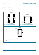
74HC595; 74HCT595 NXP Semiconductors 8-bit serial-in, serial or parallel-out shift register with output latches; 3-state (1 6+&3 67&3 4 & ' ' 4 4 2( PQD PQD Logic symbol Fig 3. 67$*( ' IEC logic symbol 67$*(6 72 ' 4 67$*( 4 ' 4 6 4 )) )) &3 4 '6 5 4 4 Fig 2.
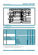
74HC595; 74HCT595 NXP Semiconductors 8-bit serial-in, serial or parallel-out shift register with output latches; 3-state 6. Pinning information 6.1 Pinning +& +&7 4 9&& 4 4 4 '6 4 2( 4 67&3 4 6+&3 4 05 *1' +& +&7 4 6 4 4 9&& 4 4 '6 4 2( 4 67&3 4 6+&3 4 05 *1' 4 6 DDR DDR Fig 5. Pin configuration DIP16, SO16 Fig 6.
74HC595; 74HCT595 NXP Semiconductors 8-bit serial-in, serial or parallel-out shift register with output latches; 3-state 6.2 Pin description Table 2.
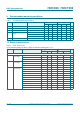
74HC595; 74HCT595 NXP Semiconductors 8-bit serial-in, serial or parallel-out shift register with output latches; 3-state 6+&3 '6 67&3 05 2( = VWDWH 4 = VWDWH 4 = VWDWH 4 = VWDWH 4 4 6 PQD Fig 8. Timing diagram 8. Limiting values Table 4. Limiting values In accordance with the Absolute Maximum Rating System (IEC 60134). Voltages are referenced to GND (ground = 0 V). Symbol Parameter VCC supply voltage Conditions Min Max Unit 0.5 +7 V IIK input clamping current VI < 0.
4HC595; 74HCT595 NXP Semiconductors 8-bit serial-in, serial or parallel-out shift register with output latches; 3-state 9. Recommended operating conditions Table 5. Recommended operating conditions Symbol Parameter VCC supply voltage Conditions 74HC595 74HCT595 Unit Min Typ Max Min Typ Max 2.0 5.0 6.0 4.5 5.0 5.5 V VI input voltage 0 - VCC 0 - VCC V VO output voltage 0 - VCC 0 - VCC V t/V input transition rise and fall rate VCC = 2.
74HC595; 74HCT595 NXP Semiconductors 8-bit serial-in, serial or parallel-out shift register with output latches; 3-state Table 6. Static characteristics …continued At recommended operating conditions; voltages are referenced to GND (ground = 0 V). Symbol VOL Parameter LOW-level output voltage 40 C to +85 C Conditions 40 C to +125 C Unit Min Typ Max Min Max IO = 20 A; VCC = 2.0 V - 0 0.1 - 0.1 V IO = 20 A; VCC = 4.5 V - 0 0.1 - 0.1 V IO = 20 A; VCC = 6.0 V - 0 0.
74HC595; 74HCT595 NXP Semiconductors 8-bit serial-in, serial or parallel-out shift register with output latches; 3-state Table 6. Static characteristics …continued At recommended operating conditions; voltages are referenced to GND (ground = 0 V). Symbol Parameter 40 C to +85 C Conditions 40 C to +125 C Min Typ Max Min Max Unit IOZ OFF-state output current VI = VIH or VIL; VCC = 5.5 V; VO = VCC or GND - - 5.0 - 10 A ICC supply current VI = VCC or GND; IO = 0 A; VCC = 5.
74HC595; 74HCT595 NXP Semiconductors 8-bit serial-in, serial or parallel-out shift register with output latches; 3-state Table 7. Dynamic characteristics …continued Voltages are referenced to GND (ground = 0 V); for test circuit see Figure 14. Symbol Parameter tW pulse width 25 C Conditions 40 C to +85 C 40 C to +125 C Unit Min Typ[1] Max Min Max Min Max VCC = 2 V 75 17 - 95 - 110 - ns VCC = 4.
74HC595; 74HCT595 NXP Semiconductors 8-bit serial-in, serial or parallel-out shift register with output latches; 3-state Table 7. Dynamic characteristics …continued Voltages are referenced to GND (ground = 0 V); for test circuit see Figure 14.
74HC595; 74HCT595 NXP Semiconductors 8-bit serial-in, serial or parallel-out shift register with output latches; 3-state 12. Waveforms IPD[ 9, 6+&3 LQSXW 90 *1' W: W 3+/ W 3/+ 92+ 90 4 6 RXWSXW 92/ PQD Measurement points are given in Table 8. VOL and VOH are typical output voltage levels that occur with the output load. Fig 9.
74HC595; 74HCT595 NXP Semiconductors 8-bit serial-in, serial or parallel-out shift register with output latches; 3-state 9, 90 6+&3 LQSXW *1' W VX W VX WK WK 9, 90 '6 LQSXW *1' 92+ 90 4 6 RXWSXW 92/ PQD Measurement points are given in Table 8. The shaded areas indicate when the input is permitted to change for predictable output performance. VOL and VOH are typical output voltage levels that occur with the output load. Fig 11.
74HC595; 74HCT595 NXP Semiconductors 8-bit serial-in, serial or parallel-out shift register with output latches; 3-state WU WI 90 2( LQSXW W3/= W3=/ 4Q RXWSXW 90 /2: WR 2)) 2)) WR /2: W3+= W3=+ 4Q RXWSXW 90 +,*+ WR 2)) 2)) WR +,*+ RXWSXWV HQDEOHG RXWSXWV HQDEOHG RXWSXWV GLVDEOHG PVD Measurement points are given in Table 8. VOL and VOH are typical output voltage levels that occur with the output load. Fig 13. Enable and disable times Table 8.
74HC595; 74HCT595 NXP Semiconductors 8-bit serial-in, serial or parallel-out shift register with output latches; 3-state 9, W: QHJDWLYH SXOVH 90 9 WI WU WU WI 9, SRVLWLYH SXOVH 9 90 90 90 W: 9&& 9&& * 9, 92 5/ 6 RSHQ '87 &/ 57 DDG Test data is given in Table 9. Definitions for test circuit: CL = load capacitance including jig and probe capacitance. RL = load resistance.
74HC595; 74HCT595 NXP Semiconductors 8-bit serial-in, serial or parallel-out shift register with output latches; 3-state 13.
74HC595; 74HCT595 NXP Semiconductors 8-bit serial-in, serial or parallel-out shift register with output latches; 3-state 62 SODVWLF VPDOO RXWOLQH SDFNDJH OHDGV ERG\ ZLGWK PP 627 ' ( $ ; F \ + ( Y 0 $ = 4 $ $ $ $ SLQ LQGH[ ș / S / H Z 0 E S GHWDLO ; PP VFDOH ',0(16,216 LQFK GLPHQVLRQV DUH GHULYHG IURP WKH RULJLQDO PP GLPHQVLRQV 81,7 $ PD[ $ $ $ E S F ' ( H + ( /
74HC595; 74HCT595 NXP Semiconductors 8-bit serial-in, serial or parallel-out shift register with output latches; 3-state 6623 SODVWLF VKULQN VPDOO RXWOLQH SDFNDJH OHDGV ERG\ ZLGWK PP ' 627 ( $ ; F \ + ( Y 0 $ = 4 $ $ $ $ SLQ LQGH[ ș / S / GHWDLO ; Z 0 E S H PP VFDOH ',0(16,216 PP DUH WKH RULJLQDO GLPHQVLRQV 81,7 $ PD[ $ $ $ E S F ' ( H + ( / / S 4 Y Z \
74HC595; 74HCT595 NXP Semiconductors 8-bit serial-in, serial or parallel-out shift register with output latches; 3-state 76623 SODVWLF WKLQ VKULQN VPDOO RXWOLQH SDFNDJH OHDGV ERG\ ZLGWK PP ' 627 ( $ ; F \ + ( Y 0 $ = 4 $ SLQ LQGH[ $ $ $ ș / S / H GHWDLO ; Z 0 E S PP VFDOH ',0(16,216 PP DUH WKH RULJLQDO GLPHQVLRQV 81,7 $ PD[ $ $ $ E S F ' ( H + ( / / S 4 Y
74HC595; 74HCT595 NXP Semiconductors 8-bit serial-in, serial or parallel-out shift register with output latches; 3-state '+94)1 SODVWLF GXDO LQ OLQH FRPSDWLEOH WKHUPDO HQKDQFHG YHU\ WKLQ TXDG IODW SDFNDJH QR OHDGV 627 WHUPLQDOV ERG\ [ [ PP % ' $ $ $ ( F GHWDLO ; WHUPLQDO LQGH[ DUHD WHUPLQDO LQGH[ DUHD & H H E \ \ & Y 0 & $ % Z 0 & / (K H 'K ; PP VFDOH ',0(16,216 PP D
74HC595; 74HCT595 NXP Semiconductors 8-bit serial-in, serial or parallel-out shift register with output latches; 3-state 14. Abbreviations Table 10. Abbreviations Acronym Abbreviation CMOS Complementary Metal Oxide Semiconductor DUT Device Under Test ESD ElectroStatic Discharge HBM Human Body Model LSTTL Low-power Schottky Transistor-Transistor Logic MM Machine Model 15. Revision history Table 11.
74HC595; 74HCT595 NXP Semiconductors 8-bit serial-in, serial or parallel-out shift register with output latches; 3-state 16. Legal information 16.1 Data sheet status Document status[1][2] Product status[3] Definition Objective [short] data sheet Development This document contains data from the objective specification for product development. Preliminary [short] data sheet Qualification This document contains data from the preliminary specification.
74HC595; 74HCT595 NXP Semiconductors 8-bit serial-in, serial or parallel-out shift register with output latches; 3-state Export control — This document as well as the item(s) described herein may be subject to export control regulations. Export might require a prior authorization from competent authorities. Non-automotive qualified products — Unless this data sheet expressly states that this specific NXP Semiconductors product is automotive qualified, the product is not suitable for automotive use.
74HC595; 74HCT595 NXP Semiconductors 8-bit serial-in, serial or parallel-out shift register with output latches; 3-state 18. Contents 1 2 3 4 5 6 6.1 6.2 7 8 9 10 11 12 13 14 15 16 16.1 16.2 16.3 16.4 17 18 General description . . . . . . . . . . . . . . . . . . . . . . 1 Features and benefits . . . . . . . . . . . . . . . . . . . . 1 Applications . . . . . . . . . . . . . . . . . . . . . . . . . . . . 1 Ordering information . . . . . . . . . . . . . . . . . . . . . 2 Functional diagram . . . . . . . .