
Datasheet


74HC_HCT595_Q100 All information provided in this document is subject to legal disclaimers. © NXP B.V. 2013. All rights reserved.
Product data sheet Rev. 2 — 10 April 2013 13 of 23
NXP Semiconductors
74HC595-Q100; 74HCT595-Q100
8-bit serial-in, serial or parallel-out shift register with output latches;
3-state
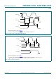
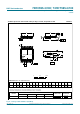
Measurement points are given in Table 8.
V
OL
and V
OH
are typical output voltage levels that occur with the output load.
Fig 10. Storage clock to output propagation delays
mna558
STCP
input
Q
n output
t
PLH
t
PHL
t
W
t
su
1/f
max
V
M
V
OH
V
I
GND
V
OL
V
M
SHCP
input
V
I
GND
V
M
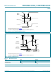
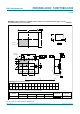
Measurement points are given in Table 8.
The shaded areas indicate when the input is permitted to change for predictable output performance.
V
OL
and V
OH
are typical output voltage levels that occur with the output load.
Fig 11. Data set-up and hold times
mna560
GND
GND
t
h
t
su
t
h
t
su
V
M
V
M
V
M
V
I
V
OH
V
OL
V
I
Q7S output
SH
CP input
D
S input