74HC75 Quad bistable transparant latch Rev. 03 — 12 November 2004 Product data sheet 1. General description The 74HC75 is a high-speed Si-gate CMOS device and is pin compatible with low power Schottky TTL (LSTTL). The 74HC75 is specified in compliance with JEDEC standard no. 7A. The 74HC75 has four bistable latches. The two latches are simultaneously controlled by one of two active HIGH enable inputs (LE12 and LE34). When LEnn is HIGH, the data enters the latches and appears at the nQ outputs.
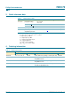
74HC75 Philips Semiconductors Quad bistable transparant latch 3. Quick reference data Table 1: Quick reference data Symbol Parameter Conditions tPHL, tPLH propagation delay CL = 15 pF; VCC = 5 V Max Unit nD to nQ, nQ - 11 - ns - 11 - ns - 3.5 - pF - 42 - pF power dissipation capacitance per latch CPD Typ LEnn to nQ, nQ input capacitance CI [1] Min VI = GND to VCC [1] CPD is used to determine the dynamic power dissipation (PD in µW).
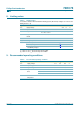
74HC75 Philips Semiconductors Quad bistable transparant latch 5. Functional diagram 2 13 1D LE12 D Q 1Q 1Q CP 16 1 L1 3 2D D Q 2Q 2Q CP 13 15 LE12 2 14 3 L2 1Q 1D 1Q 2Q 2D 2Q 16 1 15 14 L1,2 6 4 3D LE34 D Q 3Q 3Q CP L3,4 10 11 7 D 7 3Q 3D 3Q 4Q 4D 4Q L3 4D 6 LE34 4 Q 4Q 4Q CP 10 11 9 8 001aab851 9 8 L4 001aab853 Fig 1. Functional diagram 9397 750 13816 Product data sheet Fig 2. Logic symbol © Koninklijke Philips Electronics N.V. 2004.
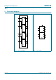
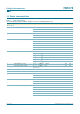
74HC75 Philips Semiconductors Quad bistable transparant latch 1D D CP LE12 13 1Q 1Q LATCH 1 C1 16 2 Q 1D 2D D Q 2Q 1 CP 15 2Q 3 14 4 LATCH 2 C1 3D D Q 3Q 9 7 1D CP LE34 8 3Q LATCH 3 10 6 11 001aab852 4D D Q CP LATCH 4 Fig 3. IEC logic symbol 4Q 4Q 001aab854 Fig 4. Logic diagram 6. Pinning information 6.1 Pinning 1Q 1 16 1Q 1D 2 15 2Q 2D 3 14 2Q LE34 4 13 LE12 75 VCC 5 12 GND 3D 6 11 3Q 4D 7 10 3Q 4Q 8 9 4Q 001aab850 Fig 5.
74HC75 Philips Semiconductors Quad bistable transparant latch 6.
74HC75 Philips Semiconductors Quad bistable transparant latch 8. Limiting values Table 5: Limiting values In accordance with the Absolute Maximum Rating System (IEC 60134). Voltages are referenced to GND (ground = 0 V). Symbol Parameter Conditions Min Max Unit VCC supply voltage IIK input diode current VI < −0.5 V or VI > VCC + 0.5 V −0.5 +7 V - ±20 mA IOK output diode current VO < −0.5 V or VO > VCC + 0.5 V - ±20 mA IO output source or sink current VO = −0.5 V to VCC + 0.
4HC75 Philips Semiconductors Quad bistable transparant latch 10. Static characteristics Table 7: Static characteristics At recommended operating conditions; voltages are referenced to GND (ground = 0 V). Symbol Parameter Conditions Min Typ Max Unit Tamb = 25 °C VIH VIL VOH VOL HIGH-level input voltage LOW-level input voltage HIGH-level output voltage LOW-level output voltage VCC = 2.0 V 1.5 1.2 - V VCC = 4.5 V 3.15 2.4 - V VCC = 6.0 V 4.2 3.2 - V VCC = 2.0 V - 0.8 0.
74HC75 Philips Semiconductors Quad bistable transparant latch Table 7: Static characteristics …continued At recommended operating conditions; voltages are referenced to GND (ground = 0 V). Symbol Parameter Conditions Min Typ Max Unit VOL LOW-level output voltage VI = VIH or VIL IO = 20 µA; VCC = 2.0 V - - 0.1 V IO = 20 µA; VCC = 4.5 V - - 0.1 V IO = 20 µA; VCC = 6.0 V - - 0.1 V IO = 4 mA; VCC = 4.5 V - - 0.33 V IO = 5.2 mA; VCC = 6.0 V - - 0.
74HC75 Philips Semiconductors Quad bistable transparant latch 11. Dynamic characteristics Table 8: Dynamic characteristics GND = 0 V; tr = tf = 6 ns; CL = 50 pF; unless otherwise specified, see Figure 10. Symbol Parameter Conditions Min Typ Max Unit propagation delay nD to nQ see Figure 6 VCC = 2.0 V - 33 110 ns VCC = 4.5 V - 12 22 ns VCC = 6.0 V - 10 19 ns VCC = 5.0 V; CL = 15 pF - 11 - ns VCC = 2.0 V - 39 120 ns VCC = 4.
74HC75 Philips Semiconductors Quad bistable transparant latch Table 8: Dynamic characteristics …continued GND = 0 V; tr = tf = 6 ns; CL = 50 pF; unless otherwise specified, see Figure 10. Symbol CPD Parameter power dissipation capacitance per latch Conditions Min Typ Max Unit - 42 - pF VCC = 2.0 V - - 140 ns VCC = 4.5 V - - 28 ns VCC = 6.0 V - - 24 ns VCC = 2.0 V - - 150 ns VCC = 4.5 V - - 30 ns VCC = 6.0 V - - 26 ns VCC = 2.0 V - - 150 ns VCC = 4.
74HC75 Philips Semiconductors Quad bistable transparant latch Table 8: Dynamic characteristics …continued GND = 0 V; tr = tf = 6 ns; CL = 50 pF; unless otherwise specified, see Figure 10.
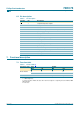
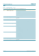
74HC75 Philips Semiconductors Quad bistable transparant latch 12. Waveforms nD input VM tPHL nQ output tPLH VM tTHL tTLH 001aab855 VM = 0.5 × VI. Fig 6. Waveforms showing the data input (nD) to output (nQ) propagation delays and the output transition times nD input VM tPHL nQ output tPLH VM tTHL tTLH 001aab856 VM = 0.5 × VI. Fig 7.
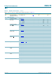
74HC75 Philips Semiconductors Quad bistable transparant latch nD input LEnn input VM tW tPHL VM nQ output tPLH nQ output tPLH tTHL tPHL tTLH VM tTLH tTHL 001aab857 VM = 0.5 × VI. Fig 9. Waveforms showing the latch enable input (LEnn) pulse width, the latch enable input to outputs (nQ, nQ) propagation delays and the output transition times VCC PULSE GENERATOR VI VO D.U.T. RT CL mna101 Test data is given in Table 9.
74HC75 Philips Semiconductors Quad bistable transparant latch 13. Package outline DIP16: plastic dual in-line package; 16 leads (300 mil) SOT38-4 ME seating plane D A2 A A1 L c e Z w M b1 (e 1) b b2 MH 9 16 pin 1 index E 1 8 0 5 10 mm scale DIMENSIONS (inch dimensions are derived from the original mm dimensions) UNIT A max. A1 min. A2 max. b b1 b2 c D (1) E (1) e e1 L ME MH w Z (1) max. mm 4.2 0.51 3.2 1.73 1.30 0.53 0.38 1.25 0.85 0.36 0.23 19.50 18.
74HC75 Philips Semiconductors Quad bistable transparant latch SO16: plastic small outline package; 16 leads; body width 3.9 mm SOT109-1 D E A X c y HE v M A Z 16 9 Q A2 A (A 3) A1 pin 1 index θ Lp 1 L 8 e 0 detail X w M bp 2.5 5 mm scale DIMENSIONS (inch dimensions are derived from the original mm dimensions) UNIT A max. A1 A2 A3 bp c D (1) E (1) e HE L Lp Q v w y Z (1) mm 1.75 0.25 0.10 1.45 1.25 0.25 0.49 0.36 0.25 0.19 10.0 9.8 4.0 3.8 1.27 6.2 5.
74HC75 Philips Semiconductors Quad bistable transparant latch SSOP16: plastic shrink small outline package; 16 leads; body width 5.3 mm D SOT338-1 E A X c y HE v M A Z 9 16 Q A2 A (A 3) A1 pin 1 index θ Lp L 8 1 detail X w M bp e 0 2.5 5 mm scale DIMENSIONS (mm are the original dimensions) UNIT A max. A1 A2 A3 bp c D (1) E (1) e HE L Lp Q v w y Z (1) θ mm 2 0.21 0.05 1.80 1.65 0.25 0.38 0.25 0.20 0.09 6.4 6.0 5.4 5.2 0.65 7.9 7.6 1.25 1.03 0.63 0.9 0.
74HC75 Philips Semiconductors Quad bistable transparant latch TSSOP16: plastic thin shrink small outline package; 16 leads; body width 4.4 mm SOT403-1 E D A X c y HE v M A Z 9 16 Q (A 3) A2 A A1 pin 1 index θ Lp L 1 8 e detail X w M bp 0 2.5 5 mm scale DIMENSIONS (mm are the original dimensions) UNIT A max. A1 A2 A3 bp c D (1) E (2) e HE L Lp Q v w y Z (1) θ mm 1.1 0.15 0.05 0.95 0.80 0.25 0.30 0.19 0.2 0.1 5.1 4.9 4.5 4.3 0.65 6.6 6.2 1 0.75 0.
74HC75 Philips Semiconductors Quad bistable transparant latch 14. Revision history Table 10: Revision history Document ID Release date Data sheet status Change notice Doc. number 74HC75_3 20041112 - Modifications: Product data sheet Supersedes 9397 750 13816 74HC_HCT75_CNV_2 • The format of this data sheet has been redesigned to comply with the current presentation and information standard of Philips Semiconductors. • • Removed type number 74HCT75. Inserted family specification.
74HC75 Philips Semiconductors Quad bistable transparant latch 15. Data sheet status Level Data sheet status [1] Product status [2] [3] Definition I Objective data Development This data sheet contains data from the objective specification for product development. Philips Semiconductors reserves the right to change the specification in any manner without notice. II Preliminary data Qualification This data sheet contains data from the preliminary specification.
74HC75 Philips Semiconductors Quad bistable transparant latch 19. Contents 1 2 3 4 5 6 6.1 6.2 7 7.1 8 9 10 11 12 13 14 15 16 17 18 General description . . . . . . . . . . . . . . . . . . . . . . 1 Features . . . . . . . . . . . . . . . . . . . . . . . . . . . . . . . 1 Quick reference data . . . . . . . . . . . . . . . . . . . . . 2 Ordering information . . . . . . . . . . . . . . . . . . . . . 2 Functional diagram . . . . . . . . . . . . . . . . . . . . . . 3 Pinning information . . . . . . . . . . .