
Datasheet

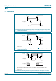

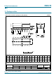


Table Of Contents
- 1. General description
- 2. Features
- 3. Quick reference data
- 4. Ordering information
- 5. Functional diagram
- 6. Pinning information
- 7. Functional description
- 8. Limiting values
- 9. Recommended operating conditions
- 10. Static characteristics
- 11. Dynamic characteristics
- 12. Waveforms
- 13. Package outline
- 14. Revision history
- 15. Data sheet status
- 16. Definitions
- 17. Disclaimers
- 18. Contact information
- 19. Contents

9397 750 13816 © Koninklijke Philips Electronics N.V. 2004. All rights reserved.
Product data sheet Rev. 03 — 12 November 2004 13 of 20
Philips Semiconductors
74HC75
Quad bistable transparant latch
V
M
= 0.5 × V
I
.
Fig 9. Waveforms showing the latch enable input (LEnn) pulse width, the latch enable
input to outputs (nQ, n
Q) propagation delays and the output transition times
Test data is given in Table 9.
Definitions for test circuit:
R
T
= Termination resistance should be equal to output impedance Z
o
of the pulse generator.
C
L
= Load capacitance including jig and probe capacitance.
Fig 10. Load circuitry for switching times
Table 9: Test data
Supply Input Load
V
CC
V
I
t
r
, t
f
C
L
2.0 V V
CC
6 ns 50 pF
4.5 V V
CC
6 ns 50 pF
6.0 V V
CC
6 ns 50 pF
5.0 V V
CC
6 ns 15 pF
nD input
LEnn input
nQ output
nQ output
t
W
V
M
V
M
V
M
001aab857
t
PHL
t
PLH
t
THL
t
TLH
t
THL
t
PLH
t
PHL
t
TLH
mna101
V
CC
V
I
V
O
R
T
C
L
PULSE
GENERATOR
D.U.T.