
Datasheet


74HC_HCT08 All information provided in this document is subject to legal disclaimers. © NXP B.V. 2012. All rights reserved.
Product data sheet Rev. 4 — 6 September 2012 2 of 16
NXP Semiconductors
74HC08; 74HCT08
Quad 2-input AND gate
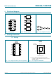
4. Functional diagram
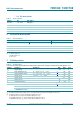
5. Pinning information
5.1 Pinning
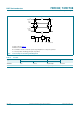
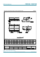
Fig 1. Logic symbol Fig 2. IEC logic symbol Fig 3. Logic diagram (one gate)
mna222
1A
1B
1Y
2
1
3
2A
2B
2Y
5
4
6
3A
3B
3Y
10
9
8
4A
4B
4Y
13
12
11
mna223
3
&
&
&
&
2
1
6
5
4
8
10
9
11
13
12
mna221
A
B
Y
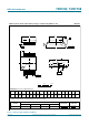
(1) The die substrate is attached to this pad using
conductive die attach material. It cannot be used as a
supply pin or input.
Fig 4. Pin configuration DIP14, SO14 and (T)SSOP14 Fig 5. Pin configuration DHVQFN14
$ 9
&&
% %
< $
$ <
% %
< $
*1
' <
+&
+&7
DDD
*1'
7UDQVSDUHQWWRSYLHZ
<
$
%
%
$
<
<
$
%
%
*1'
<
$
9
&&
WHUP
LQDO
LQGH[DUHD
+&
+&7
DDD