
Datasheet


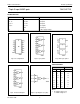
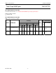
Table Of Contents

December 1990 2
Philips Semiconductors Product specification
Triple 3-input NAND gate 74HC/HCT10
FEATURES
• Output capability: standard
• I
CC
category: SSI
GENERAL DESCRIPTION
The 74HC/HCT10 are high-speed Si-gate CMOS devices and are pin compatible with low power Schottky TTL (LSTTL).
They are specified in compliance with JEDEC standard no. 7A.
The 74HC/HCT10 provide the 3-input NAND function.
QUICK REFERENCE DATA
GND = 0 V; T
amb
=25°C; t
r
=t
f
= 6 ns
Notes
1. C
PD
is used to determine the dynamic power dissipation (P
D
in µW):
P
D
=C
PD
× V
CC
2
× f
i
+ ∑ (C
L
× V
CC
2
× f
O
) where:
f
i
= input frequency in MHz
f
o
= output frequency in MHz
C
L
= output load capacitance in pF
V
CC
= supply voltage in V
∑ (C
L
× V
CC
2
× f
o
) = sum of outputs
2. For HC the condition is V
I
= GND to V
CC
For HCT the condition is V
I
= GND to V
CC
− 1.5 V.
ORDERING INFORMATION
See
“74HC/HCT/HCU/HCMOS Logic Package Information”
.
SYMBOL PARAMETER CONDITIONS
TYPICAL
UNIT
HC HCT
t
PHL
/ t
PLH
propagation delay nA, nB, nC to nY C
L
= 15 pF; V
CC
=5V 9 11 ns
C
I
input capacitance 3.5 3.5 pF
C
PD
power dissipation capacitance per gate notes 1 and 2 12 14 pF