
Datasheet

74HC_HCT125 All information provided in this document is subject to legal disclaimers. © NXP Semiconductors N.V. 2015. All rights reserved.
Product data sheet Rev. 5 — 19 January 2015 3 of 17
NXP Semiconductors
74HC125; 74HCT125
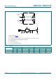
Quad buffer/line driver; 3-state
5.2 Pin description
6. Functional description
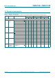
[1] H = HIGH voltage level; L = LOW voltage level; X = don’t care; Z = high-impedance OFF-state.
7. Limiting values
[1] The input and output voltage ratings may be exceeded if the input and output current ratings are observed.
[2] For DIP14 package: P
tot
derates linearly with 12 mW/K above 70 C.
For SO14 package: P
tot
derates linearly with 8 mW/K above 70 C.
For (T)SSOP14 packages: P
tot
derates linearly with 5.5 mW/K above 60 C.
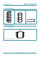
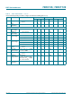
Table 2. Pin description
Symbol Pin Description
1OE
, 2OE, 3OE, 4OE 1, 4, 10, 13 output enable input (active LOW)
1A, 2A, 3A, 4A 2, 5, 9, 12 data input
1Y, 2Y, 3Y, 4Y 3, 6, 8, 11 data output
GND 7 ground (0 V)
V
CC
14 supply voltage
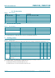
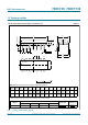
Table 3. Function table
[1]
Control Input Output
nOE nA nY
LLL
HH
HXZ
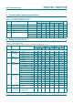
Table 4. Limiting values
In accordance with the Absolute Maximum Rating System (IEC 60134). Voltages are referenced to GND (ground = 0 V).
Symbol Parameter Conditions Min Max Unit
V
CC
supply voltage 0.5 +7 V
I
IK
input clamping current V
I
< 0.5 V or V
I
>V
CC
+0.5 V
[1]
- 20 mA
I
OK
output clamping current V
O
< 0.5 V or V
O
>V
CC
+0.5V
[1]
- 20 mA
I
O
output current V
O
= 0.5 V to (V
CC
+0.5V) - 35 mA
I
CC
supply current - +70 mA
I
GND
ground current - 70 mA
T
stg
storage temperature 65 +150 C
P
tot
total power dissipation
[2]
DIP14 package - 750 mW
SO14 and (T)SSOP14
packages
- 500 mW