
Datasheet

74HC_HCT125 All information provided in this document is subject to legal disclaimers. © NXP Semiconductors N.V. 2015. All rights reserved.
Product data sheet Rev. 5 — 19 January 2015 7 of 17
NXP Semiconductors
74HC125; 74HCT125
Quad buffer/line driver; 3-state
[1] t
pd
is the same as t
PLH
and t
PHL
.
[2] t
en
is the same as t
PZH
and t
PZL
.
[3] t
dis
is the same as t
PLZ
and t
PHZ
.
[4] t
t
is the same as t
THL
and t
TLH
.
[5] C
PD
is used to determine the dynamic power dissipation (P
D
in W).
P
D
=C
PD
V
CC
2
f
i
N+(C
L
V
CC
2
f
o
) where:
f
i
= input frequency in MHz;
f
o
= output frequency in MHz;
C
L
= output load capacitance in pF;
V
CC
= supply voltage in V;
N = number of inputs switching;
(C
L
V
CC
2
f
o
) = sum of outputs.
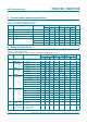
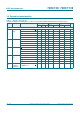
11. Waveforms
74HCT125
t
pd
propagation
delay
nA to nY; see Figure 5
[1]
V
CC
= 4.5 V - 15 25 - 31 - 38 ns
V
CC
=5V; C
L
=15pF - 12 - - - - - ns
t
en
enable time nOE to nY; see Figure 6
[2]
V
CC
= 4.5 V - 15 28 - 35 - 42 ns
t
dis
disable time nOE to nY; see Figure 6
[3]
V
CC
= 4.5 V - 15 25 - 31 - 38 ns
t
t
transition
time
nY; see Figure 5
[4]
- 5 12 - 15 - 18 ns
C
PD
power
dissipation
capacitance
C
L
=50pF;f=1 MHz;
V
I
=GNDtoV
CC
1.5 V
[5]
-24- - - - -pF
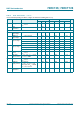
Table 7. Dynamic characteristics
…continued
Voltages are referenced to GND (ground = 0 V); C
L
= 50 pF unless otherwise specified; for test circuit see Figure 7.
Symbol Parameter Conditions 25 C 40 C to +85 C 40 C to +125 C Unit
Min Typ Max Min Max Min Max
Measurement points are given in Table 8.
V
OL
and V
OH
are typical voltage output levels that occur with the output load.
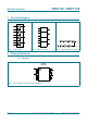
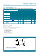
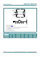
Fig 5. Propagation delay input (nA) to output (nY)
Q$
LQSXW
Q<
RXWSXW
9
,
9
0
9
0
9
0
9
0
*1'
9
2+
9
2/
W
7+/
W
7/+
W
3+/
W
3/+
DDD