
Datasheet


74HC_HCT166 All information provided in this document is subject to legal disclaimers. © NXP B.V. 2013. All rights reserved.
Product data sheet Rev. 3 — 11 September 2013 4 of 21
NXP Semiconductors
74HC166; 74HCT166
8-bit parallel-in/serial out shift register
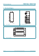
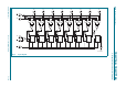
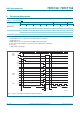
5. Pinning information
5.1 Pinning
5.2 Pin description
Fig 5. Pin configuration (DIP16, SO16 and (T)SSOP16)
74HC166
74HCT166
DS V
CC
D0 PE
D1 D7
D2 Q7
D3 D6
CE D5
CP D4
GND MR
aaa-008815
1
2
3
4
5
6
7
8
10
9
12
11
14
13
16
15
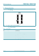
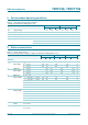
Table 2. Pin description
Symbol Pin Description
DS 1 serial data input
D0 to D7 2, 3, 4, 5, 10, 11, 12, 14 parallel data inputs
CE
6 clock enable input (active LOW)
CP 7 clock input (LOW-to-HIGH edge-triggered)
GND 8 ground (0 V)
MR
9 asynchronous master reset (active LOW)
Q7 13 serial output from the last stage
PE
15 parallel enable input (active LOW)
V
CC
16 positive supply voltage