
Datasheet


74HC_HCT166 All information provided in this document is subject to legal disclaimers. © NXP B.V. 2013. All rights reserved.
Product data sheet Rev. 3 — 11 September 2013 5 of 21
NXP Semiconductors
74HC166; 74HCT166
8-bit parallel-in/serial out shift register
6. Functional description
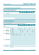
[1] H = HIGH voltage level;
h = HIGH voltage level one set-up time prior to the LOW-to-HIGH clock transition;
L = LOW voltage level;
l = LOW voltage level one set-up time prior to the LOW-to-HIGH clock transition;
q = state of the referenced output one set-up time prior to the LOW-to-HIGH clock transition;
X = don’t care;
= LOW-to-HIGH clock transition.
Table 3. Function table
[1]
Operating modes Inputs Qn registers Output
PE CE CP DS D0 to D7 Q0 Q1 to Q6 Q7
parallel load I I X I L L to L L
II X h H H to H H
serial shift h I l X L q0 to q5 q6
hI h X H q0 to q5 q6
hold “do nothing”XHXXXq0q1 to q6q7
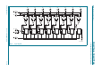
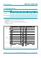
Fig 6. Typical clear, shift, load, inhibit, and shift sequences
H
L
H
L
H
L
H
H
load
aaa-008820clear
CP
MR
DS
shift/
load
D0
D1
D2
D3
D4
D5
D6
D7
Q7
CE
mode
control
inputs
parallel
inputs
output
inhibit
serial shiftserial shift
HH
L
HHH
LL