
Datasheet


74HC_HCT175 All information provided in this document is subject to legal disclaimers. © NXP Semiconductors N.V. 2014. All rights reserved.
Product data sheet Rev. 4 — 8 April 2014 4 of 19
NXP Semiconductors
74HC175; 74HCT175
Quad D-type flip-flop with reset; positive-edge trigger
6. Functional description
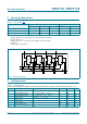
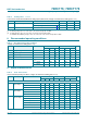
[1] H = HIGH voltage level;
h = HIGH voltage level one set-up time prior to the LOW-to-HIGH clock transition;
L = LOW voltage level;
l = LOW voltage level one set-up time prior to the LOW-to-HIGH clock transition;
X = don’t care;
= LOW-to-HIGH clock transition.
7. Limiting values
Table 3. Function table
[1]
Operating modes Inputs Outputs
MR CP Dn Qn Qn
reset (clear) L X X L H
load “1” H hHL
load “0” H lLH
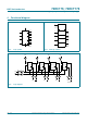
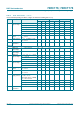
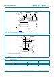
Fig 7. Functional diagram
DDD
4
5'
&3
44 44 44
4
4
''''
05
4
))
'
&3
4
5'
4
))
'
&3
4
5'
4
))
'
&3
4
5'
4
))
'
&3
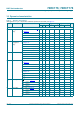
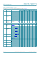
Table 4. Limiting values
In accordance with the Absolute Maximum Rating System (IEC 60134). Voltages are referenced to GND (ground = 0 V)
Symbol Parameter Conditions Min Max Unit
V
CC
supply voltage 0.5 +7 V
I
IK
input clamping current V
I
< 0.5 V or V
I
>V
CC
+0.5V - 20 mA
I
OK
output clamping current V
O
< 0.5 V or V
O
>V
CC
+0.5V - 20 mA
I
O
output current 0.5 V < V
O
< V
CC
+0.5V - 25 mA
I
CC
supply current - 50 mA
I
GND
ground current 50 - mA
T
stg
storage temperature 65 +150 C