
Datasheet

74HC_HCT193 All information provided in this document is subject to legal disclaimers. © NXP B.V. 2013. All rights reserved.
Product data sheet Rev. 4 — 24 June 2013 19 of 30
NXP Semiconductors
74HC193; 74HCT193
Presettable synchronous 4-bit binary up/down counter
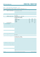
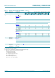
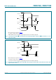
Measurement points are given in Tabl e 1 0.
t
PLH
and t
PHL
are the same as t
pd
.
Logic levels V
OL
and V
OH
are typical output voltage levels that occur with the output load.
Fig 11. The parallel load input (PL) and data (Dn) to Qn output propagation delays and PL removal time to clock
input (CPU, CPD)
001aag415
Dn input
V
I
GND
V
I
GND
V
I
GND
V
OH
V
OL
Qn output
CPU, CPD
input
PL input V
M
V
M
V
M
V
M
t
W
t
rec
t
PLH
t
PHL
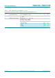
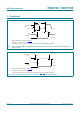
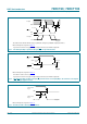
Measurement points are given in Tabl e 1 0.
t
PLH
and t
PHL
are the same as t
pd
.
Logic levels V
OL
and V
OH
are typical output voltage levels that occur with the output load.
Fig 12. The master reset input (MR) pulse width, MR to Qn propagation delays, MR to CPU, CPD removal time and
output transition times
001aag416
MR input
Qn output
V
OH
V
OL
V
I
GND
V
I
GND
CPU, CPD
input
V
M
V
M
V
M
10 %
90 %
t
rec
t
PHL
t
THL
t
W
t
TLH