
Datasheet


74HC_HCT1G86_4 © NXP B.V. 2007. All rights reserved.
Product data sheet Rev. 04 — 20 July 2007 5 of 11
NXP Semiconductors
74HC1G86; 74HCT1G86
2-input EXCLUSIVE-OR gate
11. Dynamic characteristics
[1] t
pd
is the same as t
PLH
and t
PHL
.
[2] C
PD
is used to determine the dynamic power dissipation P
D
(µW).
P
D
=C
PD
× V
CC
2
× f
i
+ ∑ (C
L
× V
CC
2
× f
o
) where:
f
i
= input frequency in MHz
f
o
= output frequency in MHz
C
L
= output load capacitance in pF
V
CC
= supply voltage in Volts
∑ (C
L
× V
CC
2
× f
o
) = sum of outputs
I
CC
supply current V
I
=V
CC
or GND; I
O
=0A;
V
CC
= 5.5 V
- - 10 - 20 µA
∆I
CC
additional supply
current
per input; V
CC
= 4.5 V to 5.5 V;
V
I
=V
CC
− 2.1 V; I
O
=0A
- - 500 - 850 µA
C
I
input capacitance - 1.5 - - - pF
Table 7. Static characteristics
…continued
Voltages are referenced to GND (ground = 0 V). All typical values are measured at T
amb
=25
°
C.
Symbol Parameter Conditions −40 °C to +85 °C −40 °C to +125 °C Unit
Min Typ Max Min Max
Table 8. Dynamic characteristics
GND = 0 V; t
r
= t
f
≤
6.0 ns; All typical values are measured at T
amb
=25
°
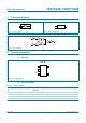
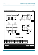
C. For test circuit see Figure 6
Symbol Parameter Conditions −40 °C to +85 °C −40 °C to +125 °C Unit
Min Typ Max Min Max
For type 74HC1G86
t
pd
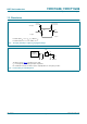
propagation delay A and B to Y; see Figure 5
[1]
V
CC
= 2.0 V; C
L
= 50 pF - 22 115 - 135 ns
V
CC
= 4.5 V; C
L
= 50 pF - 11 23 - 27 ns
V
CC
= 5.0 V; C
L
=15pF - 9 - - - ns
V
CC
= 6.0 V; C
L
=50pF - 9 20 - 23 ns
C
PD
power dissipation
capacitance
V
I
= GND to V
CC
[2]
-23- - -pF
For type 74HCT1G86
t
pd
propagation delay A and B to Y; see Figure 5
[1]
V
CC
= 4.5 V; C
L
= 50 pF - 13 23 - 27 ns
V
CC
= 5.0 V; C
L
=15pF - 10 - - - ns
C
PD
power dissipation
capacitance
V
I
= GND to V
CC
− 1.5 V
[2]
-23- - -pF