
Datasheet


74HC_HCT1G86_4 © NXP B.V. 2007. All rights reserved.
Product data sheet Rev. 04 — 20 July 2007 6 of 11
NXP Semiconductors
74HC1G86; 74HCT1G86
2-input EXCLUSIVE-OR gate
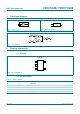
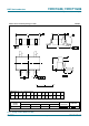
12. Waveforms
For 74HC1G86: V
M
= 0.5 × V
CC
; V
I
= GND to V
CC
.
For 74HCT1G86: V
M
= 1.3 V; V
I
= GND to 3.0 V.
Fig 5. The input (A and B) to output (Y) propagation delays
mna041
t
PHL
t
PLH
V
M
V
M
A, B
input
Y
output
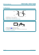
Test data is given in Table 8. Definitions for test circuit:
C
L
= Load capacitance including jig and probe capacitance.
R
T
= Termination resistance should be equal to output impedance Z
o
of the pulse generator.
Fig 6. Load circuitry for switching times
V
CC
V
I
V
O
mna034
DUT
C
L
50 pF
R
T
PULSE
GENERATOR