
Datasheet


74HC_HCT244 All information provided in this document is subject to legal disclaimers. © NXP B.V. 2012. All rights reserved.
Product data sheet Rev. 4 — 24 September 2012 7 of 18
NXP Semiconductors
74HC244; 74HCT244
Octal buffer/line driver; 3-state
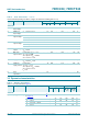
[1] t
pd
is the same as t
PHL
and t
PLH
.
[2] t
en
is the same as t
PZH
and t
PZL
.
[3] t
dis
is the same as t
PHZ
and t
PLZ
.
[4] t
t
is the same as t
THL
and t
TLH
.
[5] C
PD
is used to determine the dynamic power dissipation (P
D
in W):
P
D
=C
PD
V
CC
2
f
i
N+ (C
L
V
CC
2
f
o
) where:
f
i
= input frequency in MHz;
f
o
= output frequency in MHz;
C
L
= output load capacitance in pF;
V
CC
= supply voltage in V;
N = number of inputs switching;
(C
L
V
CC
2
f
o
) = sum of outputs.
t
en
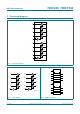
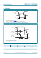
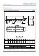
enable time nOE to nYn; see Figure 7
[2]
V
CC
= 2.0 V - 36 150 190 225 ns
V
CC
= 4.5 V - 13 30 38 45 ns
V
CC
= 6.0 V - 10 26 33 38 ns
t
dis
disable time nOE to nYn or see Figure 7
[3]
V
CC
= 2.0 V - 39 150 190 225 ns
V
CC
= 4.5 V - 14 30 38 45 ns
V
CC
= 6.0 V - 11 26 33 38 ns
t
t
transition time see Figure 6
[4]
V
CC
= 2.0 V - 14 60 75 90 ns
V
CC
= 4.5 V - 5 12 15 18 ns
V
CC
= 6.0 V - 4 10 13 15 ns
C
PD
power dissipation
capacitance
per buffer; V
I
=GNDtoV
CC
[5]
-35- - -pF
74HCT244
t
pd
propagation delay nAn to nYn;
see Figure 6
[1]
V
CC
= 4.5 V - 13 22 28 33 ns
V
CC
= 5.0 V; C
L
=15pF - 11 - - - ns
t
en
enable time nOE to nYn; V
CC
= 4.5 V; see
Figure 7
[2]
-153038 45ns
t
dis
disable time nOE to nYn; V
CC
= 4.5 V; see
Figure 7
[3]
-152531 38ns
t
t
transition time V
CC
= 4.5 V; see Figure 6
[4]
- 5 12 15 18 ns
C
PD
power dissipation
capacitance
per buffer;
V
I
=GNDtoV
CC
1.5 V
[5]
-35- - -pF
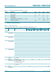
Table 7. Dynamic characteristics
…continued
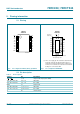
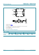
GND = 0 V; for load circuit see Figure 8.
Symbol Parameter Conditions 25 C 40 C to +125 C Unit
Min Typ Max Max
(85 C)
Max
(125 C)