
Datasheet


74HC_HCT273 All information provided in this document is subject to legal disclaimers. © NXP B.V. 2013. All rights reserved.
Product data sheet Rev. 4 — 10 June 2013 10 of 21
NXP Semiconductors
74HC273; 74HCT273
Octal D-type flip-flop with reset; positive-edge trigger
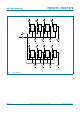
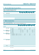
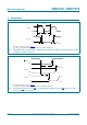
11. Waveforms
Measurement points are given in Table 8.
V
OL
and V
OH
are typical voltage output levels that occur with the output load.
Fig 7. Propagation delay clock input (CP) to output (Qn), clock (CP) pulse width, output transition time and the
maximum clock pulse frequency
001aae062
CP input
Qn
output
t
PHL
t
PLH
t
W
t
W
V
M
10%
90%
V
OH
V
I
GND
V
OL
V
M
V
M
1/f
max
t
THL
t
TLH
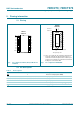
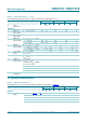
Measurement points are given in Table 8.
V
OL
and V
OH
are typical voltage output levels that occur with the output load.
Fig 8. Propagation delay master reset (MR) to output (Qn), pulse width master reset (MR) and recovery time
master reset (MR) to clock (CP)
mna464
MR
input
CP
input
Qn
output
t
PHL
t
W
t
rec
V
M
V
I
GND
V
I
V
OL
GND
V
M
V
M
V
OH