
Datasheet


74HC_HCT273 All information provided in this document is subject to legal disclaimers. © NXP B.V. 2013. All rights reserved.
Product data sheet Rev. 4 — 10 June 2013 4 of 21
NXP Semiconductors
74HC273; 74HCT273
Octal D-type flip-flop with reset; positive-edge trigger
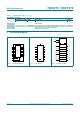
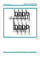
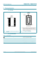
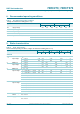
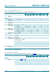
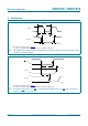
5. Pinning information
5.1 Pinning
5.2 Pin description
(1) This is not a supply pin. The substrate is attached to this
pad using conductive die attach material. There is no
electrical or mechanical requirement to solder this pad.
However, if it is soldered, the solder land should remain
floating or be connected to GND.
Fig 5. Pin configuration DIP20, SO20, SSOP20 and
TSSOP20
Fig 6. Pin configuration DHVQFN20
74HC273
74HCT273
MR V
CC
Q0 Q7
D0 D7
D1 D6
Q1 Q6
Q2 Q5
D2 D5
D3 D4
Q3 Q4
GND CP
001aae053
1
2
3
4
5
6
7
8
9
10
12
11
14
13
16
15
18
17
20
19
001aae054
74HC273
74HCT273
Transparent top view
Q4
D3
Q3
D4
D2 D5
Q2 Q5
Q1 Q6
D1 D6
D0 D7
Q0 Q7
GND
CP
MR
V
CC
9
12
8 13
7 14
6 15
5 16
4 17
3 18
2 19
10
11
1
20
terminal 1
index area
GND
(1)
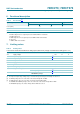
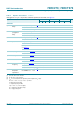
Table 2. Pin description
Symbol Pin Description
MR
1 master reset input (active LOW)
Q0, Q1, Q2, Q3, Q4, Q5, Q6, Q7 2, 5, 6, 9, 12, 15, 16, 19 flip-flop output
D0, D1, D2, D3, D4, D5, D6, D7 3, 4, 7, 8, 13, 14, 17, 18 data input
GND 10 ground (0 V)
CP 11 clock input (LOW-to-HIGH, edge-triggered)
V
CC
20 supply voltage