
Datasheet


74HC_HCT273 All information provided in this document is subject to legal disclaimers. © NXP B.V. 2013. All rights reserved.
Product data sheet Rev. 4 — 10 June 2013 7 of 21
NXP Semiconductors
74HC273; 74HCT273
Octal D-type flip-flop with reset; positive-edge trigger
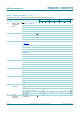
10. Dynamic characteristics
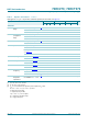
C
I
input
capacitance
-3.5- - - - -pF
74HCT273
V
IH
HIGH-level
input voltage
V
CC
= 4.5 V to 5.5 V 2.0 1.6 - 2.0 - 2.0 - V
V
IL
LOW-level
input voltage
V
CC
= 4.5 V to 5.5 V - 1.2 0.8 - 0.8 - 0.8 V
V
OH
HIGH-level
output voltage
V
I
= V
IH
or V
IL
; V
CC
= 4.5 V
I
O
= 20 A 4.4 4.5 - 4.4 - 4.4 - V
I
O
= 4.0 mA 3.98 4.32 - 3.84 - 3.7 - V
V
OL
LOW-level
output voltage
V
I
= V
IH
or V
IL
; V
CC
= 4.5 V
I
O
= 20 A; V
CC
= 4.5 V - 0 0.1 - 0.1 - 0.1 V
I
O
= 5.2 mA; V
CC
= 5.5 V - 0.15 0.26 - 0.33 - 0.4 V
I
I
input leakage
current
V
I
= V
CC
or GND;
V
CC
=5.5V
--0.1 - 1-1 A
I
CC
supply current V
I
= V
CC
or GND; I
O
=0A;
V
CC
=5.5V
- - 8.0 - 80 - 160 A
I
CC
additional
supply current
per input pin;
V
I
=V
CC
2.1 V;
other inputs at V
CC
or GND;
V
CC
= 4.5 V to 5.5 V
MR
input - 100 360 - 450 - 490 A
CP input - 175 630 - 787.5 - 857.5 A
Dn input - 15 54 - 67.5 - 73.5 A
C
I
input
capacitance
-3.5- - - - -pF
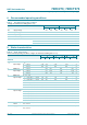
Table 6. Static characteristics
…continued
At recommended operating conditions; voltages are referenced to GND (ground = 0 V).
Symbol Parameter Conditions 25 C 40 C to +85 C 40 C to +125 C Unit
Min Typ Max Min Max Min Max
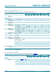
Table 7. Dynamic characteristics
GND (ground = 0 V); C
L
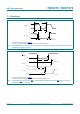
= 50 pF unless otherwise specified; for test circuit, see Figure 10
Symbol Parameter Conditions 25 C 40 C to +85 C 40 C to +125 C Unit
Min Typ Max Min Max Min Max
74HC273
t
pd
propagation
delay
CP to Qn; see Figure 7
[1]
V
CC
= 2.0 V - 41 150 - 185 - 225 ns
V
CC
= 4.5 V - 15 30 - 37 - 45 ns
V
CC
= 5.0 V; C
L
=15pF - 15 - - - - - ns
V
CC
= 6.0 V - 13 26 - 31 - 38 ns